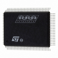
ST92F150CV1QB STMicroelectronics, ST92F150CV1QB Datasheet - Page 339

ST92F150CV1QB
Manufacturer Part Number
ST92F150CV1QB
Description
MCU 8BIT 128K FLASH 100PQFP
Manufacturer
STMicroelectronics
Series
ST9r
Datasheet
1.ST92F150CV1TB.pdf
(429 pages)
Specifications of ST92F150CV1QB
Core Processor
ST9
Core Size
8/16-Bit
Speed
24MHz
Connectivity
CAN, I²C, LIN, SCI, SPI
Peripherals
DMA, LVD, POR, PWM, WDT
Number Of I /o
77
Program Memory Size
128KB (128K x 8)
Program Memory Type
FLASH
Eeprom Size
1K x 8
Ram Size
4K x 8
Voltage - Supply (vcc/vdd)
4.5 V ~ 5.5 V
Data Converters
A/D 16x10b
Oscillator Type
Internal
Operating Temperature
-40°C ~ 105°C
Package / Case
100-QFP
Processor Series
ST92F15x
Core
ST9
Data Bus Width
8 bit, 16 bit
Data Ram Size
6 KB
Interface Type
CAN, I2C, SCI, SPI
Maximum Clock Frequency
24 MHz
Number Of Programmable I/os
80
Number Of Timers
5 x 16 bit
Operating Supply Voltage
4.5 V to 5.5 V
Maximum Operating Temperature
+ 105 C
Mounting Style
SMD/SMT
Development Tools By Supplier
ST92F150-EPB
Minimum Operating Temperature
- 40 C
On-chip Adc
16 bit x 10 bit
Lead Free Status / RoHS Status
Lead free / RoHS Compliant
Other names
497-4882
Available stocks
Company
Part Number
Manufacturer
Quantity
Price
Company:
Part Number:
ST92F150CV1QB
Manufacturer:
STMicroelectronics
Quantity:
10 000
- Current page: 339 of 429
- Download datasheet (8Mb)
CONTROLLER AREA NETWORK (Cont’d)
10.10.5.7 Bit Timing
The bit timing logic monitors the serial bus-line and
performs sampling and adjustment of the sample
point by synchronizing on the start-bit edge and re-
synchronizing on the following edges.
Its operation may be explained simply by splitting
nominal bit time into three segments as follows:
– Synchronization segment (SYNC_SEG): a bit
– Bit segment 1 (BS1): defines the location of the
– Bit segment 2 (BS2): defines the location of the
Figure 152. Bit Timing
change is expected to occur within this time seg-
ment. It has a fixed length of one time quantum
(1 x t
sample point. It includes the PROP_SEG and
PHASE_SEG1 of the CAN standard. Its duration
is programmable between 1 and 16 time quanta
but may be automatically lengthened to compen-
sate for positive phase drifts due to differences in
the frequency of the various nodes of the net-
work.
transmit point. It represents the PHASE_SEG2
of the CAN standard. Its duration is programma-
ble between 1 and 8 time quanta but may also be
automatically shortened to compensate for neg-
ative phase drifts.
B
NominalBitTime
with:
t
t
t
t
BRP = BRP[5:0] + 1 = Baud Rate Prescaler
BRP[5:0] is defined in the CBTR0 Register,
TS1[3:0] and TS2[2:0] are defined in the CBTR1 Register.
CAN
BS1
BS2
CAN
CPU
audRate
SYNC_SEG
= t
= t
).
= t
= time period of the CPU clock,
1 x t
CAN
CAN
CPU
CAN
x (TS1[3:0] + 1) ,
x (TS2[2:0] + 1),
x BRP,
=
------------------------------------------------ -
NominalBitTime
=
1
1
×
BIT SEGMENT 1 (BS1)
t
CAN
+
t
BS1
t
BS1
NOMINAL BIT TIME
+
t
BS2
CONTROLLER AREA NETWORK (bxCAN)
The resynchronization jump width (RJW) defines
an upper bound to the amount of lengthening or
shortening of the bit segments. It is programmable
between 1 and 4 time quanta.
A valid edge is defined as the first transition in a bit
time from dominant to recessive bus level provid-
ed the controller itself does not send a recessive
bit.
If a valid edge is detected in BS1 instead of
SYNC_SEG, BS1 is extended by up to RJW so
that the sample point is delayed.
Conversely, if a valid edge is detected in BS2 in-
stead of SYNC_SEG, BS2 is shortened by up to
RJW so that the transmit point is moved earlier.
As a safeguard against programming errors, the
configuration of the Bit Timing Register (BTR) is
only possible while the device is in STANDBY
mode.
Note: for a detailed description of the CAN bit tim-
ing and resynchronization mechanism, please re-
fer to the ISO 11898 standard.
SAMPLE POINT
BIT SEGMENT 2 (BS2)
t
BS2
TRANSMIT POINT
339/429
9
Related parts for ST92F150CV1QB
Image
Part Number
Description
Manufacturer
Datasheet
Request
R

Part Number:
Description:
BOARD PROGRAM FOR ST92F150 MCU
Manufacturer:
STMicroelectronics
Datasheet:

Part Number:
Description:
BOARD EVALUATION FOR ST9 SERIES
Manufacturer:
STMicroelectronics
Datasheet:

Part Number:
Description:
BOARD EMULATOR FOR ST9 SERIES
Manufacturer:
STMicroelectronics
Datasheet:

Part Number:
Description:
MCU, MPU & DSP Development Tools ST9 Dedication Board
Manufacturer:
STMicroelectronics
Datasheet:

Part Number:
Description:
STMicroelectronics [RIPPLE-CARRY BINARY COUNTER/DIVIDERS]
Manufacturer:
STMicroelectronics
Datasheet:

Part Number:
Description:
STMicroelectronics [LIQUID-CRYSTAL DISPLAY DRIVERS]
Manufacturer:
STMicroelectronics
Datasheet:

Part Number:
Description:
BOARD EVAL FOR MEMS SENSORS
Manufacturer:
STMicroelectronics
Datasheet:

Part Number:
Description:
NPN TRANSISTOR POWER MODULE
Manufacturer:
STMicroelectronics
Datasheet:

Part Number:
Description:
TURBOSWITCH ULTRA-FAST HIGH VOLTAGE DIODE
Manufacturer:
STMicroelectronics
Datasheet:

Part Number:
Description:
Manufacturer:
STMicroelectronics
Datasheet:

Part Number:
Description:
DIODE / SCR MODULE
Manufacturer:
STMicroelectronics
Datasheet:

Part Number:
Description:
DIODE / SCR MODULE
Manufacturer:
STMicroelectronics
Datasheet:


