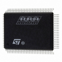
ST92F150CV1QB STMicroelectronics, ST92F150CV1QB Datasheet - Page 189

ST92F150CV1QB
Manufacturer Part Number
ST92F150CV1QB
Description
MCU 8BIT 128K FLASH 100PQFP
Manufacturer
STMicroelectronics
Series
ST9r
Datasheet
1.ST92F150CV1TB.pdf
(429 pages)
Specifications of ST92F150CV1QB
Core Processor
ST9
Core Size
8/16-Bit
Speed
24MHz
Connectivity
CAN, I²C, LIN, SCI, SPI
Peripherals
DMA, LVD, POR, PWM, WDT
Number Of I /o
77
Program Memory Size
128KB (128K x 8)
Program Memory Type
FLASH
Eeprom Size
1K x 8
Ram Size
4K x 8
Voltage - Supply (vcc/vdd)
4.5 V ~ 5.5 V
Data Converters
A/D 16x10b
Oscillator Type
Internal
Operating Temperature
-40°C ~ 105°C
Package / Case
100-QFP
Processor Series
ST92F15x
Core
ST9
Data Bus Width
8 bit, 16 bit
Data Ram Size
6 KB
Interface Type
CAN, I2C, SCI, SPI
Maximum Clock Frequency
24 MHz
Number Of Programmable I/os
80
Number Of Timers
5 x 16 bit
Operating Supply Voltage
4.5 V to 5.5 V
Maximum Operating Temperature
+ 105 C
Mounting Style
SMD/SMT
Development Tools By Supplier
ST92F150-EPB
Minimum Operating Temperature
- 40 C
On-chip Adc
16 bit x 10 bit
Lead Free Status / RoHS Status
Lead free / RoHS Compliant
Other names
497-4882
Available stocks
Company
Part Number
Manufacturer
Quantity
Price
Company:
Part Number:
ST92F150CV1QB
Manufacturer:
STMicroelectronics
Quantity:
10 000
- Current page: 189 of 429
- Download datasheet (8Mb)
MULTIFUNCTION TIMER (Cont’d)
The configuration of each input is programmed in
the Input Control Register.
Each of the two output pins can be driven from any
of three possible sources:
– Compare Register 0 logic
– Compare Register 1 logic
– Overflow/Underflow logic
Each of these three sources can cause one of the
following four actions, independently, on each of
the two outputs:
– Nop, Set, Reset, Toggle
In addition, an additional On-Chip Event signal can
be generated by two of the three sources men-
tioned above, i.e. Over/Underflow event and Com-
pare 0 event. This signal can be used internally to
Figure 102. Detailed Block Diagram
synchronise another on-chip peripheral. Five
maskable interrupt sources referring to an End Of
Count condition, 2 input captures and 2 output
compares, can generate 3 different interrupt re-
quests (with hardware fixed priority), pointing to 3
interrupt routine vectors.
Two independent DMA channels are available for
rapid data transfer operations. Each DMA request
(associated with a capture on the REG0R register,
or with a compare on the CMP0R register) has pri-
ority over an interrupt request generated by the
same source.
A SWAP mode is also available to allow high
speed continuous transfers (see Interrupt and
DMA chapter).
MULTIFUNCTION TIMER (MFT)
189/429
9
Related parts for ST92F150CV1QB
Image
Part Number
Description
Manufacturer
Datasheet
Request
R

Part Number:
Description:
BOARD PROGRAM FOR ST92F150 MCU
Manufacturer:
STMicroelectronics
Datasheet:

Part Number:
Description:
BOARD EVALUATION FOR ST9 SERIES
Manufacturer:
STMicroelectronics
Datasheet:

Part Number:
Description:
BOARD EMULATOR FOR ST9 SERIES
Manufacturer:
STMicroelectronics
Datasheet:

Part Number:
Description:
MCU, MPU & DSP Development Tools ST9 Dedication Board
Manufacturer:
STMicroelectronics
Datasheet:

Part Number:
Description:
STMicroelectronics [RIPPLE-CARRY BINARY COUNTER/DIVIDERS]
Manufacturer:
STMicroelectronics
Datasheet:

Part Number:
Description:
STMicroelectronics [LIQUID-CRYSTAL DISPLAY DRIVERS]
Manufacturer:
STMicroelectronics
Datasheet:

Part Number:
Description:
BOARD EVAL FOR MEMS SENSORS
Manufacturer:
STMicroelectronics
Datasheet:

Part Number:
Description:
NPN TRANSISTOR POWER MODULE
Manufacturer:
STMicroelectronics
Datasheet:

Part Number:
Description:
TURBOSWITCH ULTRA-FAST HIGH VOLTAGE DIODE
Manufacturer:
STMicroelectronics
Datasheet:

Part Number:
Description:
Manufacturer:
STMicroelectronics
Datasheet:

Part Number:
Description:
DIODE / SCR MODULE
Manufacturer:
STMicroelectronics
Datasheet:

Part Number:
Description:
DIODE / SCR MODULE
Manufacturer:
STMicroelectronics
Datasheet:


