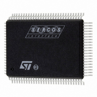
ST92F150CV1QB STMicroelectronics, ST92F150CV1QB Datasheet - Page 388

ST92F150CV1QB
Manufacturer Part Number
ST92F150CV1QB
Description
MCU 8BIT 128K FLASH 100PQFP
Manufacturer
STMicroelectronics
Series
ST9r
Datasheet
1.ST92F150CV1TB.pdf
(429 pages)
Specifications of ST92F150CV1QB
Core Processor
ST9
Core Size
8/16-Bit
Speed
24MHz
Connectivity
CAN, I²C, LIN, SCI, SPI
Peripherals
DMA, LVD, POR, PWM, WDT
Number Of I /o
77
Program Memory Size
128KB (128K x 8)
Program Memory Type
FLASH
Eeprom Size
1K x 8
Ram Size
4K x 8
Voltage - Supply (vcc/vdd)
4.5 V ~ 5.5 V
Data Converters
A/D 16x10b
Oscillator Type
Internal
Operating Temperature
-40°C ~ 105°C
Package / Case
100-QFP
Processor Series
ST92F15x
Core
ST9
Data Bus Width
8 bit, 16 bit
Data Ram Size
6 KB
Interface Type
CAN, I2C, SCI, SPI
Maximum Clock Frequency
24 MHz
Number Of Programmable I/os
80
Number Of Timers
5 x 16 bit
Operating Supply Voltage
4.5 V to 5.5 V
Maximum Operating Temperature
+ 105 C
Mounting Style
SMD/SMT
Development Tools By Supplier
ST92F150-EPB
Minimum Operating Temperature
- 40 C
On-chip Adc
16 bit x 10 bit
Lead Free Status / RoHS Status
Lead free / RoHS Compliant
Other names
497-4882
Available stocks
Company
Part Number
Manufacturer
Quantity
Price
Company:
Part Number:
ST92F150CV1QB
Manufacturer:
STMicroelectronics
Quantity:
10 000
- Current page: 388 of 429
- Download datasheet (8Mb)
ST92F124/F150/F250 - ELECTRICAL CHARACTERISTICS
EXTERNAL BUS TIMING TABLE (MC=1)
(V
Notes:
The expressions in the “Formula” column show how to calculate the typical parameter value depending on the CPU clock
period and the number of inserted wait cycles. The values in the Min column give the parameter values for a CPU clock
at 12MHz and two wait states for T1 and T2.
For certain versions of the ST92F150, the external bus has high-drive capabilities.
Legend:
Tck = INTCLK period = OSCIN period when OSCIN is not divided by 2;
TckH = INTCLK high pulse width (normally = Tck/2, except when INTCLK = OSCIN, in which case it is OSCIN high pulse
width)
TckL = INTCLK low pulse width (normally = Tck/2, except when INTCLK = OSCIN, in which case it is OSCIN low pulse
width)
P = clock prescaling value (=PRS; division factor = 1+P)
Wa = wait cycles on ALE; = max (P, programmed wait cycles in EMR2, requested wait cycles with WAIT)
Wd
388/429
N°
10
11
12
13
14
15
16
17
1
1
2
3
4
5
6
7
8
9
DD
=
TsA (ALE)
ThALE (A)
TwALE
TdAz (OEN)
TdOEN(Az)
TwOEN
TwWEN
TdOEN (DR)
ThDR (OEN)
ThOEN(A)
ThWEN(A)
TvA(OEN)
TvA(WEN)
TsD (WEN)
ThWEN(DW)
TdALE (WEN)
TdALE (OEN)
= 5V ± 10%, T
wait cycles on OEN and WEN ; = max (P, programmed wait cycles in WCR, requested wait cycles with WAIT)
Symbol
= 2*OSCIN period when OSCIN is divided by 2;
=
OSCIN period / PLL factor when the PLL is enabled
A
Address Set-up Time before ALE ↓
Address Hold Time after ALE ↓
ALE High Pulse Width
Address Float (P0) to OEN ↓
P0 driven after OEN ↑
OEN Low Pulse Width
WEN Low Pulse Width
OEN ↓ to Data Valid Delay
Data hold time after OEN ↑
Address (A21:A8) hold time after OEN ↑
Address (A21:A8) hold time after WEN ↑
Address (A21:A0) valid to OEN ↑
Address (A21:A0) valid to WEN ↑
Data Set-up time before WEN ↑
Data Hold Time after WEN ↑
ALE ↑ to WEN ↑ Delay
ALE ↑ to OEN ↑ Delay
=
–
40°C to +125°C, C
Parameter
Load
= 0 to 50pF
Tck*Wa+TckH - 48
TckL - 31
Tck*Wa+TckH - 58
0
TckL - 13
Tck*Wd+TckH - 36
Tck*Wd+TckH - 36
Tck*Wd+TckH - 44
0
0
0
Tck (Wd+Wa+1.5) - 76
Tck (Wd+Wa+1.5) - 44
Tck*Wd+TckH - 158
TckL - 37
Tck (Wd+Wa+1.5) - 54
Tck (Wd+Wa+1.5) - 50
Formula
Value (see note)
Min
160
150
172
382
414
404
408
172
10
29
50
0
0
0
0
5
Max
164
Unit
ns
ns
ns
ns
ns
ns
ns
ns
ns
ns
ns
ns
ns
ns
ns
ns
ns
Related parts for ST92F150CV1QB
Image
Part Number
Description
Manufacturer
Datasheet
Request
R

Part Number:
Description:
BOARD PROGRAM FOR ST92F150 MCU
Manufacturer:
STMicroelectronics
Datasheet:

Part Number:
Description:
BOARD EVALUATION FOR ST9 SERIES
Manufacturer:
STMicroelectronics
Datasheet:

Part Number:
Description:
BOARD EMULATOR FOR ST9 SERIES
Manufacturer:
STMicroelectronics
Datasheet:

Part Number:
Description:
MCU, MPU & DSP Development Tools ST9 Dedication Board
Manufacturer:
STMicroelectronics
Datasheet:

Part Number:
Description:
STMicroelectronics [RIPPLE-CARRY BINARY COUNTER/DIVIDERS]
Manufacturer:
STMicroelectronics
Datasheet:

Part Number:
Description:
STMicroelectronics [LIQUID-CRYSTAL DISPLAY DRIVERS]
Manufacturer:
STMicroelectronics
Datasheet:

Part Number:
Description:
BOARD EVAL FOR MEMS SENSORS
Manufacturer:
STMicroelectronics
Datasheet:

Part Number:
Description:
NPN TRANSISTOR POWER MODULE
Manufacturer:
STMicroelectronics
Datasheet:

Part Number:
Description:
TURBOSWITCH ULTRA-FAST HIGH VOLTAGE DIODE
Manufacturer:
STMicroelectronics
Datasheet:

Part Number:
Description:
Manufacturer:
STMicroelectronics
Datasheet:

Part Number:
Description:
DIODE / SCR MODULE
Manufacturer:
STMicroelectronics
Datasheet:

Part Number:
Description:
DIODE / SCR MODULE
Manufacturer:
STMicroelectronics
Datasheet:


