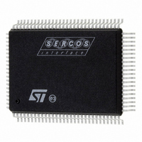
ST92F150CV1QB STMicroelectronics, ST92F150CV1QB Datasheet - Page 230

ST92F150CV1QB
Manufacturer Part Number
ST92F150CV1QB
Description
MCU 8BIT 128K FLASH 100PQFP
Manufacturer
STMicroelectronics
Series
ST9r
Datasheet
1.ST92F150CV1TB.pdf
(429 pages)
Specifications of ST92F150CV1QB
Core Processor
ST9
Core Size
8/16-Bit
Speed
24MHz
Connectivity
CAN, I²C, LIN, SCI, SPI
Peripherals
DMA, LVD, POR, PWM, WDT
Number Of I /o
77
Program Memory Size
128KB (128K x 8)
Program Memory Type
FLASH
Eeprom Size
1K x 8
Ram Size
4K x 8
Voltage - Supply (vcc/vdd)
4.5 V ~ 5.5 V
Data Converters
A/D 16x10b
Oscillator Type
Internal
Operating Temperature
-40°C ~ 105°C
Package / Case
100-QFP
Processor Series
ST92F15x
Core
ST9
Data Bus Width
8 bit, 16 bit
Data Ram Size
6 KB
Interface Type
CAN, I2C, SCI, SPI
Maximum Clock Frequency
24 MHz
Number Of Programmable I/os
80
Number Of Timers
5 x 16 bit
Operating Supply Voltage
4.5 V to 5.5 V
Maximum Operating Temperature
+ 105 C
Mounting Style
SMD/SMT
Development Tools By Supplier
ST92F150-EPB
Minimum Operating Temperature
- 40 C
On-chip Adc
16 bit x 10 bit
Lead Free Status / RoHS Status
Lead free / RoHS Compliant
Other names
497-4882
Available stocks
Company
Part Number
Manufacturer
Quantity
Price
Company:
Part Number:
ST92F150CV1QB
Manufacturer:
STMicroelectronics
Quantity:
10 000
- Current page: 230 of 429
- Download datasheet (8Mb)
MULTIPROTOCOL SERIAL COMMUNICATIONS INTERFACE (SCI-M)
MULTIPROTOCOL SERIAL COMMUNICATIONS INTERFACE (Cont’d)
INTERRUPT STATUS REGISTER (S_ISR)
R247 - Read/Write
Reset value: undefined
Bit 7 = OE: Overrun Error Pending.
This bit is set by hardware if the data in the Receiv-
er Buffer Register was not read by the CPU before
the next character was transferred into the Receiv-
er Buffer Register (the previous data is lost).
0: No Overrun Error.
1: Overrun Error occurred.
Bit 6 = FE: Framing Error Pending bit.
This bit is set by hardware if the received data
word did not have a valid stop bit.
0: No Framing Error.
1: Framing Error occurred.
Note: In the case where a framing error occurs
when the SCI is programmed in address mode
and is monitoring an address, the interrupt is as-
serted and the corrupted data element is trans-
ferred to the Receiver Buffer Register.
Bit 5 = PE: Parity Error Pending.
This bit is set by hardware if the received word did
not have the correct even or odd parity bit.
0: No Parity Error.
1: Parity Error occurred.
Bit 4 = RXAP: Receiver Address Pending.
RXAP is set by hardware after an interrupt ac-
knowledged in the address mode.
0: No interrupt in address mode.
1: Interrupt in address mode occurred.
230/429
9
OE
7
FE
PE
RXAP RXBP RXDP TXBEM
TXSEM
0
Note: The source of this interrupt is given by the
couple of bits (AMEN, AM) as detailed in the IDPR
register description.
Bit 3 = RXBP: Receiver Break Pending bit.
This bit is set by hardware if the received data in-
put is held low for the full word transmission time
(start bit, data bits, parity bit, stop bit).
0: No break received.
1: Break event occurred.
Bit 2 = RXDP: Receiver Data Pending bit.
This bit is set by hardware when data is loaded
into the Receiver Buffer Register.
0: No data received.
1: Data received in Receiver Buffer Register.
Bit 1 = TXBEM: Transmitter Buffer Register Emp-
ty.
This bit is set by hardware if the Buffer Register is
empty.
0: No Buffer Register Empty event.
1: Buffer Register Empty.
Bit 0 = TXSEM: Transmitter Shift Register Empty.
This bit is set by hardware if the Shift Register has
completed the transmission of the available data.
0: No Shift Register Empty event.
1: Shift Register Empty.
Note: The Interrupt Status Register bits can be re-
set but cannot be set by the user. The interrupt
source must be cleared by resetting the related bit
when executing the interrupt service routine (natu-
rally the other pending bits should not be reset).
Related parts for ST92F150CV1QB
Image
Part Number
Description
Manufacturer
Datasheet
Request
R

Part Number:
Description:
BOARD PROGRAM FOR ST92F150 MCU
Manufacturer:
STMicroelectronics
Datasheet:

Part Number:
Description:
BOARD EVALUATION FOR ST9 SERIES
Manufacturer:
STMicroelectronics
Datasheet:

Part Number:
Description:
BOARD EMULATOR FOR ST9 SERIES
Manufacturer:
STMicroelectronics
Datasheet:

Part Number:
Description:
MCU, MPU & DSP Development Tools ST9 Dedication Board
Manufacturer:
STMicroelectronics
Datasheet:

Part Number:
Description:
STMicroelectronics [RIPPLE-CARRY BINARY COUNTER/DIVIDERS]
Manufacturer:
STMicroelectronics
Datasheet:

Part Number:
Description:
STMicroelectronics [LIQUID-CRYSTAL DISPLAY DRIVERS]
Manufacturer:
STMicroelectronics
Datasheet:

Part Number:
Description:
BOARD EVAL FOR MEMS SENSORS
Manufacturer:
STMicroelectronics
Datasheet:

Part Number:
Description:
NPN TRANSISTOR POWER MODULE
Manufacturer:
STMicroelectronics
Datasheet:

Part Number:
Description:
TURBOSWITCH ULTRA-FAST HIGH VOLTAGE DIODE
Manufacturer:
STMicroelectronics
Datasheet:

Part Number:
Description:
Manufacturer:
STMicroelectronics
Datasheet:

Part Number:
Description:
DIODE / SCR MODULE
Manufacturer:
STMicroelectronics
Datasheet:

Part Number:
Description:
DIODE / SCR MODULE
Manufacturer:
STMicroelectronics
Datasheet:


