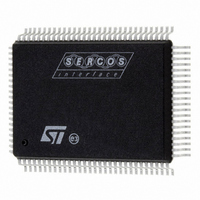
ST92F150CV1QB STMicroelectronics, ST92F150CV1QB Datasheet - Page 215

ST92F150CV1QB
Manufacturer Part Number
ST92F150CV1QB
Description
MCU 8BIT 128K FLASH 100PQFP
Manufacturer
STMicroelectronics
Series
ST9r
Datasheet
1.ST92F150CV1TB.pdf
(429 pages)
Specifications of ST92F150CV1QB
Core Processor
ST9
Core Size
8/16-Bit
Speed
24MHz
Connectivity
CAN, I²C, LIN, SCI, SPI
Peripherals
DMA, LVD, POR, PWM, WDT
Number Of I /o
77
Program Memory Size
128KB (128K x 8)
Program Memory Type
FLASH
Eeprom Size
1K x 8
Ram Size
4K x 8
Voltage - Supply (vcc/vdd)
4.5 V ~ 5.5 V
Data Converters
A/D 16x10b
Oscillator Type
Internal
Operating Temperature
-40°C ~ 105°C
Package / Case
100-QFP
Processor Series
ST92F15x
Core
ST9
Data Bus Width
8 bit, 16 bit
Data Ram Size
6 KB
Interface Type
CAN, I2C, SCI, SPI
Maximum Clock Frequency
24 MHz
Number Of Programmable I/os
80
Number Of Timers
5 x 16 bit
Operating Supply Voltage
4.5 V to 5.5 V
Maximum Operating Temperature
+ 105 C
Mounting Style
SMD/SMT
Development Tools By Supplier
ST92F150-EPB
Minimum Operating Temperature
- 40 C
On-chip Adc
16 bit x 10 bit
Lead Free Status / RoHS Status
Lead free / RoHS Compliant
Other names
497-4882
Available stocks
Company
Part Number
Manufacturer
Quantity
Price
Company:
Part Number:
ST92F150CV1QB
Manufacturer:
STMicroelectronics
Quantity:
10 000
- Current page: 215 of 429
- Download datasheet (8Mb)
MULTIPROTOCOL SERIAL COMMUNICATIONS INTERFACE (Cont’d)
10.5.4.3 Serial Expansion Mode
This mode is used to communicate with an exter-
nal synchronous peripheral.
The transmitter only provides the clock waveform
during the period that data is being transmitted on
the CLKOUT pin (the Data Envelope). Data is
latched on the rising edge of this clock.
Whenever the SCI is to receive data in serial port
expansion mode, the clock must be supplied ex-
ternally, and be synchronous with the transmitted
data. The SCI latches the incoming data on the ris-
ing edge of the received clock, which is input on
the RXCLK pin.
10.5.4.4 Synchronous Mode
This mode is used to access an external synchro-
nous peripheral, dummy start/stop bits are not in-
cluded in the data frame. Polarity, stand-by level
and active edges of I/O signals are fully and sepa-
rately programmable for both inputs and outputs.
It's necessary to set the SMEN bit of the Synchro-
nous Input Control Register (SICR) to enable this
mode and all the related extra features (otherwise
disabled).
The transmitter will provide the clock waveform
only during the period when the data is being
transmitted via the CLKOUT pin, which can be en-
abled by setting both the XTCLK and OCLK bits of
MULTIPROTOCOL SERIAL COMMUNICATIONS INTERFACE (SCI-M)
the Clock Configuration Register. Whenever the
SCI is to receive data in synchronous mode, the
clock waveform must be supplied externally via
the RXCLK pin and be synchronous with the data.
For correct receiver operation, the XRX bit of the
Clock Configuration Register must be set.
Two external signals, Request-To-Send and Data-
Carrier-Detect (RTS/DCD), can be enabled to syn-
chronise the data exchange between two serial
units. The RTS output becomes active just before
the first active edge of CLKOUT and indicates to
the target device that the MCU is about to send a
synchronous frame; it returns to its stand-by state
following the last active edge of CLKOUT (MSB
transmitted).
The DCD input can be considered as a gate that
filters RXCLK and informs the MCU that a trans-
mitting device is transmitting a data frame. Polarity
of RTS/DCD is individually programmable, as for
clocks and data.
The data word is programmable from 5 to 8 bits, as
for the other modes; parity, address/9th, stop bits
and break cannot be inserted into the transmitted
frame. Programming of the related bits of the SCI
control registers is irrelevant in Synchronous
Mode: all the corresponding interrupt requests
must, in any case, be masked in order to avoid in-
correct operation during data reception.
215/429
9
Related parts for ST92F150CV1QB
Image
Part Number
Description
Manufacturer
Datasheet
Request
R

Part Number:
Description:
BOARD PROGRAM FOR ST92F150 MCU
Manufacturer:
STMicroelectronics
Datasheet:

Part Number:
Description:
BOARD EVALUATION FOR ST9 SERIES
Manufacturer:
STMicroelectronics
Datasheet:

Part Number:
Description:
BOARD EMULATOR FOR ST9 SERIES
Manufacturer:
STMicroelectronics
Datasheet:

Part Number:
Description:
MCU, MPU & DSP Development Tools ST9 Dedication Board
Manufacturer:
STMicroelectronics
Datasheet:

Part Number:
Description:
STMicroelectronics [RIPPLE-CARRY BINARY COUNTER/DIVIDERS]
Manufacturer:
STMicroelectronics
Datasheet:

Part Number:
Description:
STMicroelectronics [LIQUID-CRYSTAL DISPLAY DRIVERS]
Manufacturer:
STMicroelectronics
Datasheet:

Part Number:
Description:
BOARD EVAL FOR MEMS SENSORS
Manufacturer:
STMicroelectronics
Datasheet:

Part Number:
Description:
NPN TRANSISTOR POWER MODULE
Manufacturer:
STMicroelectronics
Datasheet:

Part Number:
Description:
TURBOSWITCH ULTRA-FAST HIGH VOLTAGE DIODE
Manufacturer:
STMicroelectronics
Datasheet:

Part Number:
Description:
Manufacturer:
STMicroelectronics
Datasheet:

Part Number:
Description:
DIODE / SCR MODULE
Manufacturer:
STMicroelectronics
Datasheet:

Part Number:
Description:
DIODE / SCR MODULE
Manufacturer:
STMicroelectronics
Datasheet:


