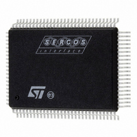
ST92F150CV1QB STMicroelectronics, ST92F150CV1QB Datasheet - Page 408

ST92F150CV1QB
Manufacturer Part Number
ST92F150CV1QB
Description
MCU 8BIT 128K FLASH 100PQFP
Manufacturer
STMicroelectronics
Series
ST9r
Datasheet
1.ST92F150CV1TB.pdf
(429 pages)
Specifications of ST92F150CV1QB
Core Processor
ST9
Core Size
8/16-Bit
Speed
24MHz
Connectivity
CAN, I²C, LIN, SCI, SPI
Peripherals
DMA, LVD, POR, PWM, WDT
Number Of I /o
77
Program Memory Size
128KB (128K x 8)
Program Memory Type
FLASH
Eeprom Size
1K x 8
Ram Size
4K x 8
Voltage - Supply (vcc/vdd)
4.5 V ~ 5.5 V
Data Converters
A/D 16x10b
Oscillator Type
Internal
Operating Temperature
-40°C ~ 105°C
Package / Case
100-QFP
Processor Series
ST92F15x
Core
ST9
Data Bus Width
8 bit, 16 bit
Data Ram Size
6 KB
Interface Type
CAN, I2C, SCI, SPI
Maximum Clock Frequency
24 MHz
Number Of Programmable I/os
80
Number Of Timers
5 x 16 bit
Operating Supply Voltage
4.5 V to 5.5 V
Maximum Operating Temperature
+ 105 C
Mounting Style
SMD/SMT
Development Tools By Supplier
ST92F150-EPB
Minimum Operating Temperature
- 40 C
On-chip Adc
16 bit x 10 bit
Lead Free Status / RoHS Status
Lead free / RoHS Compliant
Other names
497-4882
Available stocks
Company
Part Number
Manufacturer
Quantity
Price
Company:
Part Number:
ST92F150CV1QB
Manufacturer:
STMicroelectronics
Quantity:
10 000
- Current page: 408 of 429
- Download datasheet (8Mb)
ST92F124/F150/F250 - KNOWN LIMITATIONS
13 KNOWN LIMITATIONS
Limitations described in this section apply to all sil-
icon revisions. They are listed in the following ta-
ble.
Additional limitations exist on specific silicon revi-
sions identified by the following trace codes:
– ST92F124 Gxxxxxxxx1
– ST92F150 AxxxxxxxxZ
– ST92F150 AxxxxxxxxY
– ST92F250 AxxxxxxxxA
Table 74. List of limitations
13.1 FLASH ERASE SUSPEND LIMITATIONS
13.1.1 Description
In normal operation, the FSUSP bit (bit 2 in the
FCR register) must be set to suspend the current
Sector Erase operation in Flash memory in order
to access a sector not being erased. The Flash
sector erase operation is done in 3 different steps:
1. Program all addresses to 0 on selected sectors
2. Erase and erase verify
3. Reprogramming
If the erase suspend is performed during Steps 1
and 2, the flash works correctly. If the erase sus-
pend is performed during Step 3, the PGER bit (bit
408/429
1
Section 13.1
Section 13.2
Section 13.3
Section 13.4
Section 13.5
Section 13.6
Section 13.7
Section 13.8
or 1 ST92F124 xxxxx VG
or Y ST92F150 xxxxx VA
or A ST92F250 xxxxx VA
Section
“FLASH ERASE SUSPEND LIMITATIONS
“FLASH CORRUPTION WHEN EXITING STOP MODE
“I2C LIMITATIONS
“SCI-A AND CAN INTERRUPTS
“SCI-A MUTE MODE
“CAN FIFO CORRUPTION WHEN 2 FIFO MESSAGES ARE PENDING
“MFT DMA MASK BIT RESET WHEN MFT0 DMA PRIORITY LEVEL IS SET TO 0
“EMULATION CHIP LIMITATIONS
Please contact your nearest sales office for further
information.
6 in the FESR1 register) is set although no pro-
gram error occurred.
13.1.2 Workaround
After a Sector Erase suspend operation, the soft-
ware must check the status register to detect if an
erase error occurred (the corresponding sector
must be discarded). Then the software must reset
the FEERR bit. This automatically resets the flash
status register.
Whatever the state of the PGER bit at the end of
the erase operation, it will not impact the applica-
tion and an erase error is still detected.
Limitation
Related parts for ST92F150CV1QB
Image
Part Number
Description
Manufacturer
Datasheet
Request
R

Part Number:
Description:
BOARD PROGRAM FOR ST92F150 MCU
Manufacturer:
STMicroelectronics
Datasheet:

Part Number:
Description:
BOARD EVALUATION FOR ST9 SERIES
Manufacturer:
STMicroelectronics
Datasheet:

Part Number:
Description:
BOARD EMULATOR FOR ST9 SERIES
Manufacturer:
STMicroelectronics
Datasheet:

Part Number:
Description:
MCU, MPU & DSP Development Tools ST9 Dedication Board
Manufacturer:
STMicroelectronics
Datasheet:

Part Number:
Description:
STMicroelectronics [RIPPLE-CARRY BINARY COUNTER/DIVIDERS]
Manufacturer:
STMicroelectronics
Datasheet:

Part Number:
Description:
STMicroelectronics [LIQUID-CRYSTAL DISPLAY DRIVERS]
Manufacturer:
STMicroelectronics
Datasheet:

Part Number:
Description:
BOARD EVAL FOR MEMS SENSORS
Manufacturer:
STMicroelectronics
Datasheet:

Part Number:
Description:
NPN TRANSISTOR POWER MODULE
Manufacturer:
STMicroelectronics
Datasheet:

Part Number:
Description:
TURBOSWITCH ULTRA-FAST HIGH VOLTAGE DIODE
Manufacturer:
STMicroelectronics
Datasheet:

Part Number:
Description:
Manufacturer:
STMicroelectronics
Datasheet:

Part Number:
Description:
DIODE / SCR MODULE
Manufacturer:
STMicroelectronics
Datasheet:

Part Number:
Description:
DIODE / SCR MODULE
Manufacturer:
STMicroelectronics
Datasheet:


