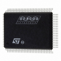
ST92F150CV1QB STMicroelectronics, ST92F150CV1QB Datasheet - Page 147

ST92F150CV1QB
Manufacturer Part Number
ST92F150CV1QB
Description
MCU 8BIT 128K FLASH 100PQFP
Manufacturer
STMicroelectronics
Series
ST9r
Datasheet
1.ST92F150CV1TB.pdf
(429 pages)
Specifications of ST92F150CV1QB
Core Processor
ST9
Core Size
8/16-Bit
Speed
24MHz
Connectivity
CAN, I²C, LIN, SCI, SPI
Peripherals
DMA, LVD, POR, PWM, WDT
Number Of I /o
77
Program Memory Size
128KB (128K x 8)
Program Memory Type
FLASH
Eeprom Size
1K x 8
Ram Size
4K x 8
Voltage - Supply (vcc/vdd)
4.5 V ~ 5.5 V
Data Converters
A/D 16x10b
Oscillator Type
Internal
Operating Temperature
-40°C ~ 105°C
Package / Case
100-QFP
Processor Series
ST92F15x
Core
ST9
Data Bus Width
8 bit, 16 bit
Data Ram Size
6 KB
Interface Type
CAN, I2C, SCI, SPI
Maximum Clock Frequency
24 MHz
Number Of Programmable I/os
80
Number Of Timers
5 x 16 bit
Operating Supply Voltage
4.5 V to 5.5 V
Maximum Operating Temperature
+ 105 C
Mounting Style
SMD/SMT
Development Tools By Supplier
ST92F150-EPB
Minimum Operating Temperature
- 40 C
On-chip Adc
16 bit x 10 bit
Lead Free Status / RoHS Status
Lead free / RoHS Compliant
Other names
497-4882
Available stocks
Company
Part Number
Manufacturer
Quantity
Price
Company:
Part Number:
ST92F150CV1QB
Manufacturer:
STMicroelectronics
Quantity:
10 000
- Current page: 147 of 429
- Download datasheet (8Mb)
EXTERNAL MEMORY SIGNALS (Cont’d)
8.2.8 WAIT: External Memory Wait
WAIT (Alternate Function Input, Active low) indi-
cates to the ST9 that the external memory requires
more time to complete the memory access cycle. If
bit EWEN (EIVR) is set, the WAIT signal is sam-
pled with the rising edge of the processor internal
clock during phase T1 or T2 of every memory cy-
cle. If the signal was sampled active, one more in-
ternal clock cycle is added to the memory cycle.
On the rising edge of the added internal clock cy-
Figure 78. External memory Read/Write sequence with external wait request (WAIT pin)
WAIT
SYSTEM
P1, P9
AS (MC=0)
ALE (MC=1)
P0
RW (MC=0)
OEN (MC=1)
WEN (MC=1)
P0
RW (MC=0)
OEN (MC=1)
WEN (MC=1)
DS (MC=0)
CLOCK
ADD.
ADD.
T1
ADDRESS
D.OUT
D.IN
ST92F124/F150/F250 - EXTERNAL MEMORY INTERFACE (EXTMI)
T2
ADDRESS
T1
ADDRESS
ADDRESS
cle, WAIT is sampled again to continue or finish
the memory cycle stretching. Note that if WAIT is
sampled active during phase T1 then AS is
stretched, while if WAIT is sampled active during
phase T2 then DS is stretched. WAIT is enabled
via software as the Alternate Function input of the
associated I/O port bit (refer to specific ST9 ver-
sion to identify the specific port and pin). Refer to
Figure
D.IN
D.OUT
T2
78.
ADD.
T1
ADD.
ADDRESS
T2
DATA OUT
D.IN
147/429
9
Related parts for ST92F150CV1QB
Image
Part Number
Description
Manufacturer
Datasheet
Request
R

Part Number:
Description:
BOARD PROGRAM FOR ST92F150 MCU
Manufacturer:
STMicroelectronics
Datasheet:

Part Number:
Description:
BOARD EVALUATION FOR ST9 SERIES
Manufacturer:
STMicroelectronics
Datasheet:

Part Number:
Description:
BOARD EMULATOR FOR ST9 SERIES
Manufacturer:
STMicroelectronics
Datasheet:

Part Number:
Description:
MCU, MPU & DSP Development Tools ST9 Dedication Board
Manufacturer:
STMicroelectronics
Datasheet:

Part Number:
Description:
STMicroelectronics [RIPPLE-CARRY BINARY COUNTER/DIVIDERS]
Manufacturer:
STMicroelectronics
Datasheet:

Part Number:
Description:
STMicroelectronics [LIQUID-CRYSTAL DISPLAY DRIVERS]
Manufacturer:
STMicroelectronics
Datasheet:

Part Number:
Description:
BOARD EVAL FOR MEMS SENSORS
Manufacturer:
STMicroelectronics
Datasheet:

Part Number:
Description:
NPN TRANSISTOR POWER MODULE
Manufacturer:
STMicroelectronics
Datasheet:

Part Number:
Description:
TURBOSWITCH ULTRA-FAST HIGH VOLTAGE DIODE
Manufacturer:
STMicroelectronics
Datasheet:

Part Number:
Description:
Manufacturer:
STMicroelectronics
Datasheet:

Part Number:
Description:
DIODE / SCR MODULE
Manufacturer:
STMicroelectronics
Datasheet:

Part Number:
Description:
DIODE / SCR MODULE
Manufacturer:
STMicroelectronics
Datasheet:


