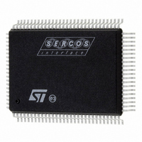
ST92F150CV1QB STMicroelectronics, ST92F150CV1QB Datasheet - Page 416

ST92F150CV1QB
Manufacturer Part Number
ST92F150CV1QB
Description
MCU 8BIT 128K FLASH 100PQFP
Manufacturer
STMicroelectronics
Series
ST9r
Datasheet
1.ST92F150CV1TB.pdf
(429 pages)
Specifications of ST92F150CV1QB
Core Processor
ST9
Core Size
8/16-Bit
Speed
24MHz
Connectivity
CAN, I²C, LIN, SCI, SPI
Peripherals
DMA, LVD, POR, PWM, WDT
Number Of I /o
77
Program Memory Size
128KB (128K x 8)
Program Memory Type
FLASH
Eeprom Size
1K x 8
Ram Size
4K x 8
Voltage - Supply (vcc/vdd)
4.5 V ~ 5.5 V
Data Converters
A/D 16x10b
Oscillator Type
Internal
Operating Temperature
-40°C ~ 105°C
Package / Case
100-QFP
Processor Series
ST92F15x
Core
ST9
Data Bus Width
8 bit, 16 bit
Data Ram Size
6 KB
Interface Type
CAN, I2C, SCI, SPI
Maximum Clock Frequency
24 MHz
Number Of Programmable I/os
80
Number Of Timers
5 x 16 bit
Operating Supply Voltage
4.5 V to 5.5 V
Maximum Operating Temperature
+ 105 C
Mounting Style
SMD/SMT
Development Tools By Supplier
ST92F150-EPB
Minimum Operating Temperature
- 40 C
On-chip Adc
16 bit x 10 bit
Lead Free Status / RoHS Status
Lead free / RoHS Compliant
Other names
497-4882
Available stocks
Company
Part Number
Manufacturer
Quantity
Price
Company:
Part Number:
ST92F150CV1QB
Manufacturer:
STMicroelectronics
Quantity:
10 000
- Current page: 416 of 429
- Download datasheet (8Mb)
ST92F124/F150/F250 - KNOWN LIMITATIONS
KNOWN LIMITATIONS (Cont’d)
Figure 3. Workaround 1 in Assembler
We can assume a time quantum number between
8 and 25. The worst case is when the baud rate
prescaler is 0 (BRP=0) and the time quantum is 8,
ie. TS1+TS2=5. This means a CPU frequency of
8MHz and 1 Mbits/sec for the CAN communica-
tion. In this case the minimum time between the
end of the acknowledge and the critical period is
52 CPU cycles (48 for the 6 bit times + 4 for the
(PROP SEG + T
code timing, we need less than 22 cycles from the
time we see the dominant state to the time we per-
form the FIFO release (one full loop + the actual
release) therefore the application will never re-
lease the FIFO at the critical time when this work-
around is implemented.
Timing analysis
- Time spent in the workaround
Inside a CAN frame, the longest period that the Rx
pin stays in recessive state is 5 bits. At the end of
the frame, the time between the acknowledge
dominant bit and the end of reception (signaled by
REC bit status) is 8T
i m u m t i m e s p e n t i n t h e w o r k a r o u n d i s :
8T
8T
416/429
1
asm (“
_whileloop: btjf r1.5, _release /* REC bit of CMSR register
_release:
“);
CANbit
CANbit
+68T
spp #48
ld
and
cp
jxnz
pushw RR232
srp
btjf
popw
+T
loop
CPU
+T
r0, R244
r0, #3
r0, #2
_release
#31
r12.3, _whileloop /* RX bit of CDGR register
or R244, #32
RR232
Seg 1
.
test
). According to the previous
CANbit
+T
release
, therefore the max-
in this case or
/*
/* set CAN0_CTRL page
/* Use spp #36 for CAN1
/* For FIFO 0
/* NB: Replace R244 with R245 for FIFO 1
/*
/*
/* (JRNE instruction)
/* if FMP is not 2 then FIFO
/* release can be done
/* push working group
/* set group F as working group
/*
/* NB: Replace R244 with R245 for FIFO 1
/* restore previous working group
set RFOM bit of CRFR register
At low speed, this time could represent a long
delay for the application, therefore it makes sense
to evaluate how frequently this delay occurs.
In order to reach the critical FMP=2, the CAN node
needs to receive 2 messages without servicing
them. Then in order to reach the critical window,
the cell has to receive a third one and the applica-
tion has to release the mailbox at the same time, at
the end of the reception.
In the application, messages are not processed
only if either the interrupt are disabled or higher
level interrupts are being serviced.
Therefore if:
T
frame
the application will never wait in the workaround
T
interrupts with a level strictly higher than the CAN
interrupt level
T
disables the CAN interrupt (or all interrupts)
T
the beginning of the CAN interrupt and the actual
location of the workaround
IT higher level
IT higher level
IT disable
IT CAN
: This is the maximum duration between
: This is the longest time the application
: This the sum of the duration of all the
+ T
IT disable
Bytes/cycles
2/4
2/4
3/6
3/6
2/6
2/8 or 10
2/4
3/6 or 10 if jmp
3/6 or 10 if jmp
3/6
2/10
+ T
IT CAN
< 2 x T
CAN
*/
*/
*/
*/
*/
*/
*/
*/
*/
*/
*/
*/
*/
*/
*/
*/
Related parts for ST92F150CV1QB
Image
Part Number
Description
Manufacturer
Datasheet
Request
R

Part Number:
Description:
BOARD PROGRAM FOR ST92F150 MCU
Manufacturer:
STMicroelectronics
Datasheet:

Part Number:
Description:
BOARD EVALUATION FOR ST9 SERIES
Manufacturer:
STMicroelectronics
Datasheet:

Part Number:
Description:
BOARD EMULATOR FOR ST9 SERIES
Manufacturer:
STMicroelectronics
Datasheet:

Part Number:
Description:
MCU, MPU & DSP Development Tools ST9 Dedication Board
Manufacturer:
STMicroelectronics
Datasheet:

Part Number:
Description:
STMicroelectronics [RIPPLE-CARRY BINARY COUNTER/DIVIDERS]
Manufacturer:
STMicroelectronics
Datasheet:

Part Number:
Description:
STMicroelectronics [LIQUID-CRYSTAL DISPLAY DRIVERS]
Manufacturer:
STMicroelectronics
Datasheet:

Part Number:
Description:
BOARD EVAL FOR MEMS SENSORS
Manufacturer:
STMicroelectronics
Datasheet:

Part Number:
Description:
NPN TRANSISTOR POWER MODULE
Manufacturer:
STMicroelectronics
Datasheet:

Part Number:
Description:
TURBOSWITCH ULTRA-FAST HIGH VOLTAGE DIODE
Manufacturer:
STMicroelectronics
Datasheet:

Part Number:
Description:
Manufacturer:
STMicroelectronics
Datasheet:

Part Number:
Description:
DIODE / SCR MODULE
Manufacturer:
STMicroelectronics
Datasheet:

Part Number:
Description:
DIODE / SCR MODULE
Manufacturer:
STMicroelectronics
Datasheet:


