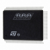
ST92F150CV1QB STMicroelectronics, ST92F150CV1QB Datasheet - Page 232

ST92F150CV1QB
Manufacturer Part Number
ST92F150CV1QB
Description
MCU 8BIT 128K FLASH 100PQFP
Manufacturer
STMicroelectronics
Series
ST9r
Datasheet
1.ST92F150CV1TB.pdf
(429 pages)
Specifications of ST92F150CV1QB
Core Processor
ST9
Core Size
8/16-Bit
Speed
24MHz
Connectivity
CAN, I²C, LIN, SCI, SPI
Peripherals
DMA, LVD, POR, PWM, WDT
Number Of I /o
77
Program Memory Size
128KB (128K x 8)
Program Memory Type
FLASH
Eeprom Size
1K x 8
Ram Size
4K x 8
Voltage - Supply (vcc/vdd)
4.5 V ~ 5.5 V
Data Converters
A/D 16x10b
Oscillator Type
Internal
Operating Temperature
-40°C ~ 105°C
Package / Case
100-QFP
Processor Series
ST92F15x
Core
ST9
Data Bus Width
8 bit, 16 bit
Data Ram Size
6 KB
Interface Type
CAN, I2C, SCI, SPI
Maximum Clock Frequency
24 MHz
Number Of Programmable I/os
80
Number Of Timers
5 x 16 bit
Operating Supply Voltage
4.5 V to 5.5 V
Maximum Operating Temperature
+ 105 C
Mounting Style
SMD/SMT
Development Tools By Supplier
ST92F150-EPB
Minimum Operating Temperature
- 40 C
On-chip Adc
16 bit x 10 bit
Lead Free Status / RoHS Status
Lead free / RoHS Compliant
Other names
497-4882
Available stocks
Company
Part Number
Manufacturer
Quantity
Price
Company:
Part Number:
ST92F150CV1QB
Manufacturer:
STMicroelectronics
Quantity:
10 000
- Current page: 232 of 429
- Download datasheet (8Mb)
MULTIPROTOCOL SERIAL COMMUNICATIONS INTERFACE (SCI-M)
MULTIPROTOCOL SERIAL COMMUNICATIONS INTERFACE (Cont’d)
INTERRUPT/DMA PRIORITY REGISTER (IDPR)
R249 - Read/Write
Reset value: undefined
Bit 7 = AMEN: Address Mode Enable.
This bit, together with the AM bit (in the CHCR reg-
ister), decodes the desired addressing/9th data
bit/character match operation.
In Address mode the SCI monitors the input serial
data until its address is detected
Note: Upon reception of address, the RXAP bit (in
the Interrupt Status Register) is set and an inter-
rupt cycle can begin. The address character will
not be transferred into the Receiver Buffer Regis-
ter but all data following the matched SCI address
and preceding the next address word will be trans-
ferred to the Receiver Buffer Register and the
proper interrupts updated. If the address does not
match, all data following this unmatched address
will not be transferred to the Receiver Buffer Reg-
ister.
In any of the cases the RXAP bit must be reset by
software before the next word is transferred into
the Buffer Register.
When AMEN is reset and AM is set, a useful char-
acter search function is performed. This allows the
SCI to generate an interrupt whenever a specific
character is encountered (e.g. Carriage Return).
Bit 6 = SB: Set Break.
0: Stop the break transmission after minimum
1: Transmit a break following the transmission of all
Note: The break will be a low level on the transmit-
ter data output for at least one complete word for-
232/429
9
AMEN
AMEN
break length.
data in the Transmitter Shift Register and the
Buffer Register.
7
0
0
1
1
SB
AM
0
1
0
1
SA
Address interrupt if 9th data bit = 1
Address interrupt if character match
Address interrupt if character match
and 9th data bit =1
Address interrupt if character match
with word immediately following Break
RXD
TXD
PRL2
PRL1
PRL0
0
mat. If software does not reset SB before the min-
imum break length has finished, the break condi-
tion will continue until software resets SB. The SCI
terminates the break condition with a high level on
the transmitter data output for one transmission
clock period.
Bit 5 = SA: Set Address.
If an address/9th data bit mode is selected, SA val-
ue will be loaded for transmission into the Shift
Register. This bit is cleared by hardware after its
load.
0: Indicate it is not an address word.
1: Indicate an address word.
Note: Proper procedure would be, when the
Transmitter Buffer Register is empty, to load the
value of SA and then load the data into the Trans-
mitter Buffer Register.
Bit 4 = RXD: Receiver DMA Mask.
This bit is reset by hardware when the transaction
counter value decrements to zero. At that time a
receiver End of Block interrupt can occur.
0: Disable Receiver DMA request (the RXDP bit in
1: Enable Receiver DMA request (the RXDP bit in
Bit 3 = TXD: Transmitter DMA Mask.
This bit is reset by hardware when the transaction
counter value decrements to zero. At that time a
transmitter End Of Block interrupt can occur.
0: Disable Transmitter DMA request (TXBEM or
1: Enable Transmitter DMA request (TXBEM or
Bit 2:0 = PRL[2:0]: SCI Interrupt/DMA Priority bits.
The priority for the SCI is encoded with
(PRL2,PRL1,PRL0). Priority level 0 is the highest,
while level 7 represents no priority.
When the user has defined a priority level for the
SCI, priorities within the SCI are hardware defined.
These SCI internal priorities are:
Receiver DMA request
Transmitter DMA request
Receiver interrupt
Transmitter interrupt
the S_ISR register can request an interrupt).
the S_ISR register can request a DMA transfer).
TXSEM bits in S_ISR can request an interrupt).
TXSEM bits in S_ISR can request a DMA trans-
fer).
highest priority
lowest priority
Related parts for ST92F150CV1QB
Image
Part Number
Description
Manufacturer
Datasheet
Request
R

Part Number:
Description:
BOARD PROGRAM FOR ST92F150 MCU
Manufacturer:
STMicroelectronics
Datasheet:

Part Number:
Description:
BOARD EVALUATION FOR ST9 SERIES
Manufacturer:
STMicroelectronics
Datasheet:

Part Number:
Description:
BOARD EMULATOR FOR ST9 SERIES
Manufacturer:
STMicroelectronics
Datasheet:

Part Number:
Description:
MCU, MPU & DSP Development Tools ST9 Dedication Board
Manufacturer:
STMicroelectronics
Datasheet:

Part Number:
Description:
STMicroelectronics [RIPPLE-CARRY BINARY COUNTER/DIVIDERS]
Manufacturer:
STMicroelectronics
Datasheet:

Part Number:
Description:
STMicroelectronics [LIQUID-CRYSTAL DISPLAY DRIVERS]
Manufacturer:
STMicroelectronics
Datasheet:

Part Number:
Description:
BOARD EVAL FOR MEMS SENSORS
Manufacturer:
STMicroelectronics
Datasheet:

Part Number:
Description:
NPN TRANSISTOR POWER MODULE
Manufacturer:
STMicroelectronics
Datasheet:

Part Number:
Description:
TURBOSWITCH ULTRA-FAST HIGH VOLTAGE DIODE
Manufacturer:
STMicroelectronics
Datasheet:

Part Number:
Description:
Manufacturer:
STMicroelectronics
Datasheet:

Part Number:
Description:
DIODE / SCR MODULE
Manufacturer:
STMicroelectronics
Datasheet:

Part Number:
Description:
DIODE / SCR MODULE
Manufacturer:
STMicroelectronics
Datasheet:


