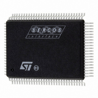
ST92F150CV1QB STMicroelectronics, ST92F150CV1QB Datasheet - Page 260

ST92F150CV1QB
Manufacturer Part Number
ST92F150CV1QB
Description
MCU 8BIT 128K FLASH 100PQFP
Manufacturer
STMicroelectronics
Series
ST9r
Datasheet
1.ST92F150CV1TB.pdf
(429 pages)
Specifications of ST92F150CV1QB
Core Processor
ST9
Core Size
8/16-Bit
Speed
24MHz
Connectivity
CAN, I²C, LIN, SCI, SPI
Peripherals
DMA, LVD, POR, PWM, WDT
Number Of I /o
77
Program Memory Size
128KB (128K x 8)
Program Memory Type
FLASH
Eeprom Size
1K x 8
Ram Size
4K x 8
Voltage - Supply (vcc/vdd)
4.5 V ~ 5.5 V
Data Converters
A/D 16x10b
Oscillator Type
Internal
Operating Temperature
-40°C ~ 105°C
Package / Case
100-QFP
Processor Series
ST92F15x
Core
ST9
Data Bus Width
8 bit, 16 bit
Data Ram Size
6 KB
Interface Type
CAN, I2C, SCI, SPI
Maximum Clock Frequency
24 MHz
Number Of Programmable I/os
80
Number Of Timers
5 x 16 bit
Operating Supply Voltage
4.5 V to 5.5 V
Maximum Operating Temperature
+ 105 C
Mounting Style
SMD/SMT
Development Tools By Supplier
ST92F150-EPB
Minimum Operating Temperature
- 40 C
On-chip Adc
16 bit x 10 bit
Lead Free Status / RoHS Status
Lead free / RoHS Compliant
Other names
497-4882
Available stocks
Company
Part Number
Manufacturer
Quantity
Price
Company:
Part Number:
ST92F150CV1QB
Manufacturer:
STMicroelectronics
Quantity:
10 000
- Current page: 260 of 429
- Download datasheet (8Mb)
SERIAL PERIPHERAL INTERFACE (SPI)
SERIAL PERIPHERAL INTERFACE (Cont’d)
10.7.6 Register Description
DATA REGISTER (SPDR)
R240 - Read/Write
Register Page: 7
Reset Value: 0000 0000 (00h)
The SPDR register is used to transmit and receive
data on the serial bus. In the master device only a
write to this register will initiate transmission/re-
ception of another byte.
Notes: During the last clock cycle the SPIF bit is
set, a copy of the received data byte in the shift
register is moved to a buffer. When the user reads
the serial peripheral data register, the buffer is ac-
tually being read.
Warning: A write to the SPDR register places data
directly into the shift register for transmission.
A read to the SPDR register returns the value lo-
cated in the buffer and not the content of the shift
register (see
CONTROL REGISTER (SPCR)
R241 - Read/Write
Register Page: 7
Reset Value: 0000 0000 (00h)
Bit 7 = SPIE Serial peripheral interrupt enable.
This bit is set and cleared by software.
0: Interrupt is inhibited
1: An SPI interrupt is generated whenever either
Bit 6 = SPOE Serial peripheral output enable.
This bit is set and cleared by software. It is also
cleared by hardware when, in master mode, SS=0
(see
0: SPI alternate functions disabled (MISO, MOSI
1: SPI alternate functions enabled (MISO, MOSI
260/429
9
SPIE
D7
SPIF or MODF are set in the SPSR register
while the other flag is 0.
and SCK can only work as input)
and SCK can work as input or output depending
on the value of MSTR)
7
7
Section 10.7.4.5 Master Mode
SPOE SPIS MSTR
D6
Figure
D5
121).
D4
CPOL
D3
CPHA
D2
Fault).
SPR1
D1
D0
SPR0
0
0
Note: To use the MISO, MOSI and SCK alternate
functions (input or output), the corresponding I/O
port must be programmed as alternate function
output.
Bit 5 = SPIS Interrupt Selection.
This bit is set and cleared by software.
0: Interrupt source is external interrupt
1: Interrupt source is SPI
Bit 4 = MSTR Master.
This bit is set and cleared by software. It is also
cleared by hardware when, in master mode, SS=0
(see
0: Slave mode is selected
1: Master mode is selected, the function of the
Bit 3 = CPOL Clock polarity.
This bit is set and cleared by software. This bit de-
termines the steady state of the serial Clock. The
CPOL bit affects both the master and slave
modes.
0: The steady state is a low value at the SCK pin.
1: The steady state is a high value at the SCK pin.
Bit 2 = CPHA Clock phase.
This bit is set and cleared by software.
0: The first clock transition is the first data capture
1: The second clock transition is the first capture
Bit 1:0 = SPR[1:0] Serial peripheral rate.
These bits are set and cleared by software. They
select one of four baud rates to be used as the se-
rial clock when the device is a master.
These 2 bits have no effect in slave mode.
Table 49. Serial Peripheral Baud Rate
SCK pin changes from an input to an output and
the functions of the MISO and MOSI pins are re-
versed.
edge.
edge.
INTCLK Clock Divide
Section 10.7.4.5 Master Mode
16
32
2
4
SPR1
0
0
1
1
Fault).
SPR0
0
1
0
1
Related parts for ST92F150CV1QB
Image
Part Number
Description
Manufacturer
Datasheet
Request
R

Part Number:
Description:
BOARD PROGRAM FOR ST92F150 MCU
Manufacturer:
STMicroelectronics
Datasheet:

Part Number:
Description:
BOARD EVALUATION FOR ST9 SERIES
Manufacturer:
STMicroelectronics
Datasheet:

Part Number:
Description:
BOARD EMULATOR FOR ST9 SERIES
Manufacturer:
STMicroelectronics
Datasheet:

Part Number:
Description:
MCU, MPU & DSP Development Tools ST9 Dedication Board
Manufacturer:
STMicroelectronics
Datasheet:

Part Number:
Description:
STMicroelectronics [RIPPLE-CARRY BINARY COUNTER/DIVIDERS]
Manufacturer:
STMicroelectronics
Datasheet:

Part Number:
Description:
STMicroelectronics [LIQUID-CRYSTAL DISPLAY DRIVERS]
Manufacturer:
STMicroelectronics
Datasheet:

Part Number:
Description:
BOARD EVAL FOR MEMS SENSORS
Manufacturer:
STMicroelectronics
Datasheet:

Part Number:
Description:
NPN TRANSISTOR POWER MODULE
Manufacturer:
STMicroelectronics
Datasheet:

Part Number:
Description:
TURBOSWITCH ULTRA-FAST HIGH VOLTAGE DIODE
Manufacturer:
STMicroelectronics
Datasheet:

Part Number:
Description:
Manufacturer:
STMicroelectronics
Datasheet:

Part Number:
Description:
DIODE / SCR MODULE
Manufacturer:
STMicroelectronics
Datasheet:

Part Number:
Description:
DIODE / SCR MODULE
Manufacturer:
STMicroelectronics
Datasheet:


