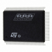
ST92F150CV1QB STMicroelectronics, ST92F150CV1QB Datasheet - Page 143

ST92F150CV1QB
Manufacturer Part Number
ST92F150CV1QB
Description
MCU 8BIT 128K FLASH 100PQFP
Manufacturer
STMicroelectronics
Series
ST9r
Datasheet
1.ST92F150CV1TB.pdf
(429 pages)
Specifications of ST92F150CV1QB
Core Processor
ST9
Core Size
8/16-Bit
Speed
24MHz
Connectivity
CAN, I²C, LIN, SCI, SPI
Peripherals
DMA, LVD, POR, PWM, WDT
Number Of I /o
77
Program Memory Size
128KB (128K x 8)
Program Memory Type
FLASH
Eeprom Size
1K x 8
Ram Size
4K x 8
Voltage - Supply (vcc/vdd)
4.5 V ~ 5.5 V
Data Converters
A/D 16x10b
Oscillator Type
Internal
Operating Temperature
-40°C ~ 105°C
Package / Case
100-QFP
Processor Series
ST92F15x
Core
ST9
Data Bus Width
8 bit, 16 bit
Data Ram Size
6 KB
Interface Type
CAN, I2C, SCI, SPI
Maximum Clock Frequency
24 MHz
Number Of Programmable I/os
80
Number Of Timers
5 x 16 bit
Operating Supply Voltage
4.5 V to 5.5 V
Maximum Operating Temperature
+ 105 C
Mounting Style
SMD/SMT
Development Tools By Supplier
ST92F150-EPB
Minimum Operating Temperature
- 40 C
On-chip Adc
16 bit x 10 bit
Lead Free Status / RoHS Status
Lead free / RoHS Compliant
Other names
497-4882
Available stocks
Company
Part Number
Manufacturer
Quantity
Price
Company:
Part Number:
ST92F150CV1QB
Manufacturer:
STMicroelectronics
Quantity:
10 000
- Current page: 143 of 429
- Download datasheet (8Mb)
8.2 EXTERNAL MEMORY SIGNALS
The access to external memory is made using the
AS, DS, RW, Port 0, Port1, Port9, DS2 and WAIT
signals described below.
Refer to
8.2.1 AS: Address Strobe
AS (Output, Active low, Tristate) is active during
the System Clock high-level phase of each T1
memory cycle: an AS rising edge indicates that
Memory Address and Read/Write Memory control
signals are valid.
AS is released in high-impedance during the bus
acknowledge cycle or under the processor control
by setting the HIMP bit (MODER.0, R235).
Under Reset, AS is held high with an internal weak
pull-up.
The behavior of this signal is also affected by the
MC, ASAF, ETO, LAS[1:0] and UAS[1:0] bits in the
EMR1 or EMR2 registers. Refer to the Register
description.
8.2.2 DS: Data Strobe
DS (Output, Active low, Tristate) is active during the
internal clock high-level phase of each T2 memory
cycle. During an external memory read cycle, the
data on Port 0 must be valid before the DS rising
edge. During an external memory write cycle, the
data on Port 0 are output on the falling edge of DS
and they are valid on the rising edge of DS. When
the internal memory is accessed DS is kept high
during the whole memory cycle.
DS is released in high-impedance during bus ac-
knowledge cycle or under processor control by set-
ting the HIMP bit (MODER.0, R235).
Under Reset status, DS is held high with an internal
weak pull-up.
The behavior of this signal is also affected by the
LDS[2:0], UDS[2:0], DS2EN and MC bits in the
Figure
76.
ST92F124/F150/F250 - EXTERNAL MEMORY INTERFACE (EXTMI)
EMR1 or WCR register. Refer to the Register de-
scription.
8.2.3 RW: Read/Write
RW (Output, Active low, Tristate) identifies the
type of memory cycle: RW=”1” identifies a memory
read cycle, RW=”0” identifies a memory write cy-
cle. It is defined at the beginning of each memory
cycle and it remains stable until the following
memory cycle.
RW is released in high-impedance during bus ac-
knowledge cycle or under processor control by
setting the HIMP bit (MODER).
Under Reset status, RW is held high with an inter-
nal weak pull-up.
The behavior of this signal is affected by the MC
and ETO bits in the EMR1 register. Refer to the
Register description.
8.2.4 DS2: Data Strobe 2
This additional Data Strobe pin (Alternate Function
Output, Active low, Tristate) allows two different
external memories to be connected to the ST9, the
upper memory block (A21=1 typically RAM) and
the lower memory block (A21=0 typically ROM)
without any external logic. The selection between
the upper and lower memory blocks depends on
the A21 address pin value.
The upper memory block is controlled by the DS
pin while the lower memory block is controlled by
the DS2 pin. When the internal memory is ad-
dressed, DS2 is kept high during the whole mem-
ory cycle. DS2 is enabled via software as the Alter-
nate Function output of the associated I/O port bit.
DS2 is released in high-impedance during bus ac-
knowledge cycle or under processor control by
setting the HIMP bit (MODER.0, r235).
The behavior of this signal is also affected by the
DS2EN bit in the EMR1 register. Refer to the Reg-
ister description.
143/429
9
Related parts for ST92F150CV1QB
Image
Part Number
Description
Manufacturer
Datasheet
Request
R

Part Number:
Description:
BOARD PROGRAM FOR ST92F150 MCU
Manufacturer:
STMicroelectronics
Datasheet:

Part Number:
Description:
BOARD EVALUATION FOR ST9 SERIES
Manufacturer:
STMicroelectronics
Datasheet:

Part Number:
Description:
BOARD EMULATOR FOR ST9 SERIES
Manufacturer:
STMicroelectronics
Datasheet:

Part Number:
Description:
MCU, MPU & DSP Development Tools ST9 Dedication Board
Manufacturer:
STMicroelectronics
Datasheet:

Part Number:
Description:
STMicroelectronics [RIPPLE-CARRY BINARY COUNTER/DIVIDERS]
Manufacturer:
STMicroelectronics
Datasheet:

Part Number:
Description:
STMicroelectronics [LIQUID-CRYSTAL DISPLAY DRIVERS]
Manufacturer:
STMicroelectronics
Datasheet:

Part Number:
Description:
BOARD EVAL FOR MEMS SENSORS
Manufacturer:
STMicroelectronics
Datasheet:

Part Number:
Description:
NPN TRANSISTOR POWER MODULE
Manufacturer:
STMicroelectronics
Datasheet:

Part Number:
Description:
TURBOSWITCH ULTRA-FAST HIGH VOLTAGE DIODE
Manufacturer:
STMicroelectronics
Datasheet:

Part Number:
Description:
Manufacturer:
STMicroelectronics
Datasheet:

Part Number:
Description:
DIODE / SCR MODULE
Manufacturer:
STMicroelectronics
Datasheet:

Part Number:
Description:
DIODE / SCR MODULE
Manufacturer:
STMicroelectronics
Datasheet:


