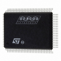
ST92F150CV1QB STMicroelectronics, ST92F150CV1QB Datasheet - Page 423

ST92F150CV1QB
Manufacturer Part Number
ST92F150CV1QB
Description
MCU 8BIT 128K FLASH 100PQFP
Manufacturer
STMicroelectronics
Series
ST9r
Datasheet
1.ST92F150CV1TB.pdf
(429 pages)
Specifications of ST92F150CV1QB
Core Processor
ST9
Core Size
8/16-Bit
Speed
24MHz
Connectivity
CAN, I²C, LIN, SCI, SPI
Peripherals
DMA, LVD, POR, PWM, WDT
Number Of I /o
77
Program Memory Size
128KB (128K x 8)
Program Memory Type
FLASH
Eeprom Size
1K x 8
Ram Size
4K x 8
Voltage - Supply (vcc/vdd)
4.5 V ~ 5.5 V
Data Converters
A/D 16x10b
Oscillator Type
Internal
Operating Temperature
-40°C ~ 105°C
Package / Case
100-QFP
Processor Series
ST92F15x
Core
ST9
Data Bus Width
8 bit, 16 bit
Data Ram Size
6 KB
Interface Type
CAN, I2C, SCI, SPI
Maximum Clock Frequency
24 MHz
Number Of Programmable I/os
80
Number Of Timers
5 x 16 bit
Operating Supply Voltage
4.5 V to 5.5 V
Maximum Operating Temperature
+ 105 C
Mounting Style
SMD/SMT
Development Tools By Supplier
ST92F150-EPB
Minimum Operating Temperature
- 40 C
On-chip Adc
16 bit x 10 bit
Lead Free Status / RoHS Status
Lead free / RoHS Compliant
Other names
497-4882
Available stocks
Company
Part Number
Manufacturer
Quantity
Price
Company:
Part Number:
ST92F150CV1QB
Manufacturer:
STMicroelectronics
Quantity:
10 000
- Current page: 423 of 429
- Download datasheet (8Mb)
KNOWN LIMITATIONS (Cont’d)
13.8 EMULATION CHIP LIMITATIONS
Additional limitations exist on Emulation chips (EMU2 emulator). These limitations correspond to those
present in AxxxxxxxxY trace codes (ST92F150). They are listed in the following table.
13.8.1
DIRECTIONAL, WEAK PULL-UP PORTS
This section applies to ports P1[7:3], P4[1], P8[7:2]
and P9[7:0].
During the reset phase (external reset signal low)
and the delay of 20400 clock periods (t
lowing a reset, these ports are in High Impedance
state, while according to the datasheet they should
Table 76. Reset Behaviour Table
Shaded areas represent erroneous operations.
Section 13.8.1
Section 13.8.2
Section 13.8.3
Section 13.8.4
Section 13.8.5
Section 13.8.6
Section 13.8.7
Section 13.8.8
Section 13.8.9
Section 13.8.10
Section 13.8.11
P1[7:3] Bi-Dir + WPU
P8[7:2] Bi-Dir + WPU
P9[7:0] Bi-Dir + WPU
P4.1
Port
Section
RESET
Bi-Dir + WPU
Datasheet
Condition
RESET BEHAVIOUR FOR BI-DIRECTIONAL, WEAK PULL-UP PORTS
HIGH DRIVE I/Os WHEN BSZ=1
ADC PARASITIC DIODE
ADC ACCURACY VS. NEGATIVE INJECTION CURRENT
I2CECCR REGISTER LIMITATION
I2C BEHAVIOUR DISTURBED DURING DMA TRANSACTIONS
MFT DMA MASK BIT RESET
DMA DATA CORRUPTED BY MFT INPUT CAPTURE
SCI-A WRONG BREAK DURATION
LIN MASTER MODE NOT PRESENT ON SCI-A
LIMITATIONS ON LQFP64 PACKAGES
BEHAVIOUR
While RESET
is low
Hi-Z
Hi-Z
Hi-Z
Hi-Z
FOR
RSPH
Port Behaviour
During next
Limitation (AxxxxxxxxY trace code)
20K Clock
) fol-
Cycles
BI-
Hi-Z
Hi-Z
Hi-Z
Hi-Z
ST92F124/F150/F250 - KNOWN LIMITATIONS
have weak pull-ups. These ports then enter Weak
Pull-up state until the user overwrites the reset
values of I/O Port Control Registers PxC0, PxC1
and PxC2.
Rev Z Behaviour
Bi-Dir + WPU
Bi-Dir + WPU
Bi-Dir + WPU
Bi-Dir + WPU
After these
20K Clock
Cycles
PxC0
Control Register Value
0
0
0
0
PxC1
0
0
0
0
PxC2
423/429
0
0
0
0
1
Related parts for ST92F150CV1QB
Image
Part Number
Description
Manufacturer
Datasheet
Request
R

Part Number:
Description:
BOARD PROGRAM FOR ST92F150 MCU
Manufacturer:
STMicroelectronics
Datasheet:

Part Number:
Description:
BOARD EVALUATION FOR ST9 SERIES
Manufacturer:
STMicroelectronics
Datasheet:

Part Number:
Description:
BOARD EMULATOR FOR ST9 SERIES
Manufacturer:
STMicroelectronics
Datasheet:

Part Number:
Description:
MCU, MPU & DSP Development Tools ST9 Dedication Board
Manufacturer:
STMicroelectronics
Datasheet:

Part Number:
Description:
STMicroelectronics [RIPPLE-CARRY BINARY COUNTER/DIVIDERS]
Manufacturer:
STMicroelectronics
Datasheet:

Part Number:
Description:
STMicroelectronics [LIQUID-CRYSTAL DISPLAY DRIVERS]
Manufacturer:
STMicroelectronics
Datasheet:

Part Number:
Description:
BOARD EVAL FOR MEMS SENSORS
Manufacturer:
STMicroelectronics
Datasheet:

Part Number:
Description:
NPN TRANSISTOR POWER MODULE
Manufacturer:
STMicroelectronics
Datasheet:

Part Number:
Description:
TURBOSWITCH ULTRA-FAST HIGH VOLTAGE DIODE
Manufacturer:
STMicroelectronics
Datasheet:

Part Number:
Description:
Manufacturer:
STMicroelectronics
Datasheet:

Part Number:
Description:
DIODE / SCR MODULE
Manufacturer:
STMicroelectronics
Datasheet:

Part Number:
Description:
DIODE / SCR MODULE
Manufacturer:
STMicroelectronics
Datasheet:


