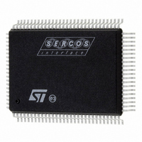
ST92F150CV1QB STMicroelectronics, ST92F150CV1QB Datasheet - Page 248

ST92F150CV1QB
Manufacturer Part Number
ST92F150CV1QB
Description
MCU 8BIT 128K FLASH 100PQFP
Manufacturer
STMicroelectronics
Series
ST9r
Datasheet
1.ST92F150CV1TB.pdf
(429 pages)
Specifications of ST92F150CV1QB
Core Processor
ST9
Core Size
8/16-Bit
Speed
24MHz
Connectivity
CAN, I²C, LIN, SCI, SPI
Peripherals
DMA, LVD, POR, PWM, WDT
Number Of I /o
77
Program Memory Size
128KB (128K x 8)
Program Memory Type
FLASH
Eeprom Size
1K x 8
Ram Size
4K x 8
Voltage - Supply (vcc/vdd)
4.5 V ~ 5.5 V
Data Converters
A/D 16x10b
Oscillator Type
Internal
Operating Temperature
-40°C ~ 105°C
Package / Case
100-QFP
Processor Series
ST92F15x
Core
ST9
Data Bus Width
8 bit, 16 bit
Data Ram Size
6 KB
Interface Type
CAN, I2C, SCI, SPI
Maximum Clock Frequency
24 MHz
Number Of Programmable I/os
80
Number Of Timers
5 x 16 bit
Operating Supply Voltage
4.5 V to 5.5 V
Maximum Operating Temperature
+ 105 C
Mounting Style
SMD/SMT
Development Tools By Supplier
ST92F150-EPB
Minimum Operating Temperature
- 40 C
On-chip Adc
16 bit x 10 bit
Lead Free Status / RoHS Status
Lead free / RoHS Compliant
Other names
497-4882
Available stocks
Company
Part Number
Manufacturer
Quantity
Price
Company:
Part Number:
ST92F150CV1QB
Manufacturer:
STMicroelectronics
Quantity:
10 000
- Current page: 248 of 429
- Download datasheet (8Mb)
ASYNCHRONOUS SERIAL COMMUNICATIONS INTERFACE (SCI-A)
ASYNCHRONOUS SERIAL COMMUNICATIONS INTERFACE (Cont’d)
DATA REGISTER (SCIDR)
R241 - Read/Write
Register Page: 26
Reset Value: Undefined
Contains the Received or Transmitted data char-
acter, depending on whether it is read from or writ-
ten to.
The Data register performs a double function (read
and write) since it is composed of two registers,
one for transmission (TDR) and one for reception
(RDR).
The TDR register provides the parallel interface
between the internal bus and the output shift reg-
ister (see
The RDR register provides the parallel interface
between the input shift register and the internal
bus (see
BAUD RATE REGISTER (SCIBRR)
R242 - Read/Write
Register Page: 26
Reset Value: 00xx xxxx (xxh)
Bits 7:6= SCP[1:0] First SCI Prescaler
These 2 prescaling bits allow several standard
clock division ranges:
248/429
9
SCP1
DR7
7
7
PR Prescaling factor
SCP0
DR6
Figure
Figure
13
SCT2
1
3
4
DR5
117).
117).
SCT1
DR4
SCT0
DR3
SCP1
SCR2 SCR1 SCR0
DR2
0
0
1
1
DR1
SCP0
0
1
0
1
DR0
0
0
Bits 5:3 = SCT[2:0] SCI Transmitter rate divisor
These 3 bits, in conjunction with the SCP1 & SCP0
bits define the total division applied to the bus
clock to yield the transmit rate clock in convention-
al Baud Rate Generator mode.
Note: This TR factor is used only when the ETPR
fine tuning factor is equal to 00h; otherwise, TR is
replaced by the (TR*ETPR) dividing factor.
Bits 2:0 = SCR[2:0] SCI Receiver rate divisor.
These 3 bits, in conjunction with the SCP1 & SCP0
bits define the total division applied to the bus
clock to yield the receive rate clock in conventional
Baud Rate Generator mode.
Note: This RR factor is used only when the ERPR
fine tuning factor is equal to 00h; otherwise, RR is
replaced by the (RR*ERPR) dividing factor.
RR Dividing Factor
TR Dividing Factor
128
128
16
32
64
16
32
64
1
2
4
8
1
2
4
8
SCR2
SCT2
0
0
0
0
1
1
1
1
0
0
0
0
1
1
1
1
SCR1
SCT1
0
0
1
1
0
0
1
1
0
0
1
1
0
0
1
1
SCR0
SCT0
0
1
0
1
0
1
0
1
0
1
0
1
0
1
0
1
Related parts for ST92F150CV1QB
Image
Part Number
Description
Manufacturer
Datasheet
Request
R

Part Number:
Description:
BOARD PROGRAM FOR ST92F150 MCU
Manufacturer:
STMicroelectronics
Datasheet:

Part Number:
Description:
BOARD EVALUATION FOR ST9 SERIES
Manufacturer:
STMicroelectronics
Datasheet:

Part Number:
Description:
BOARD EMULATOR FOR ST9 SERIES
Manufacturer:
STMicroelectronics
Datasheet:

Part Number:
Description:
MCU, MPU & DSP Development Tools ST9 Dedication Board
Manufacturer:
STMicroelectronics
Datasheet:

Part Number:
Description:
STMicroelectronics [RIPPLE-CARRY BINARY COUNTER/DIVIDERS]
Manufacturer:
STMicroelectronics
Datasheet:

Part Number:
Description:
STMicroelectronics [LIQUID-CRYSTAL DISPLAY DRIVERS]
Manufacturer:
STMicroelectronics
Datasheet:

Part Number:
Description:
BOARD EVAL FOR MEMS SENSORS
Manufacturer:
STMicroelectronics
Datasheet:

Part Number:
Description:
NPN TRANSISTOR POWER MODULE
Manufacturer:
STMicroelectronics
Datasheet:

Part Number:
Description:
TURBOSWITCH ULTRA-FAST HIGH VOLTAGE DIODE
Manufacturer:
STMicroelectronics
Datasheet:

Part Number:
Description:
Manufacturer:
STMicroelectronics
Datasheet:

Part Number:
Description:
DIODE / SCR MODULE
Manufacturer:
STMicroelectronics
Datasheet:

Part Number:
Description:
DIODE / SCR MODULE
Manufacturer:
STMicroelectronics
Datasheet:


