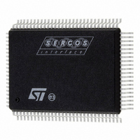
ST92F150CV1QB STMicroelectronics, ST92F150CV1QB Datasheet - Page 398

ST92F150CV1QB
Manufacturer Part Number
ST92F150CV1QB
Description
MCU 8BIT 128K FLASH 100PQFP
Manufacturer
STMicroelectronics
Series
ST9r
Datasheet
1.ST92F150CV1TB.pdf
(429 pages)
Specifications of ST92F150CV1QB
Core Processor
ST9
Core Size
8/16-Bit
Speed
24MHz
Connectivity
CAN, I²C, LIN, SCI, SPI
Peripherals
DMA, LVD, POR, PWM, WDT
Number Of I /o
77
Program Memory Size
128KB (128K x 8)
Program Memory Type
FLASH
Eeprom Size
1K x 8
Ram Size
4K x 8
Voltage - Supply (vcc/vdd)
4.5 V ~ 5.5 V
Data Converters
A/D 16x10b
Oscillator Type
Internal
Operating Temperature
-40°C ~ 105°C
Package / Case
100-QFP
Processor Series
ST92F15x
Core
ST9
Data Bus Width
8 bit, 16 bit
Data Ram Size
6 KB
Interface Type
CAN, I2C, SCI, SPI
Maximum Clock Frequency
24 MHz
Number Of Programmable I/os
80
Number Of Timers
5 x 16 bit
Operating Supply Voltage
4.5 V to 5.5 V
Maximum Operating Temperature
+ 105 C
Mounting Style
SMD/SMT
Development Tools By Supplier
ST92F150-EPB
Minimum Operating Temperature
- 40 C
On-chip Adc
16 bit x 10 bit
Lead Free Status / RoHS Status
Lead free / RoHS Compliant
Other names
497-4882
Available stocks
Company
Part Number
Manufacturer
Quantity
Price
Company:
Part Number:
ST92F150CV1QB
Manufacturer:
STMicroelectronics
Quantity:
10 000
- Current page: 398 of 429
- Download datasheet (8Mb)
ST92F124/F150/F250 - ELECTRICAL CHARACTERISTICS
I
(V
Note:
(1) Value guaranteed by design.
(2) The ST9 device must internally provide a hold time of at least 300 ns for the SDA signal in order to bridge the undefined region of the fall-
(3) The maximum hold time of the START condition has only to be met if the interface does not stretch the low period of SCL signal
Legend:
Tck = INTCLK period = Crystal Oscillator Clock period when CLOCK1 is not divided by 2;
Cb = total capacitance of one bus line in pF
FREQ[2:0] = Frequency bits value of I
I
398/429
1
2
2
Symbol
f
f
T
T
T
T
T
T
T
T
T
T
Cb
INTCLK
SCL
C/DDC-BUS TIMING TABLE
C TIMING
SDA
SCL
BUF
HIGH
LOW
HD:STA
SU:STA
HD:DAT
SU:DAT
R
F
SU:STO
DD
ing edge of SCL
= 5V ± 10%, T
P
Internal Frequency (Slave Mode)
SCL clock frequency
Bus free time between a STOP and
START condition
SCL clock high period
SCL clock low period
Hold time START condition. After this
period, the first clock pulse is generated
Set-up time for a repeated START condi-
tion
Data hold time
Data set-up time
(Without SCL stretching)
Data set-up time
(With SCL stretch-
ing)
Rise time of both SDA and SCL signals
Fall time of both SDA and SCL signals
Set-up time for STOP condition
Capacitive load for each bus line
t
BUF
S
2 x Crystal Oscillator Clock period when CLOCK1 is divided by 2;
Crystal Oscillator Clock period x PLL factor when the PLL is enabled.
A
t
HD:STA
t
=
LOW
Parameter
–
40°C to +125°C, C
2
C Own Address Register 2 (I2COAR2)
Standard Mode
Fast Mode
FREQ[2:0] = 000
FREQ[2:0] = 001
FREQ[2:0] = 010
FREQ[2:0] = 011
FREQ[2:0] = 000
FREQ[2:0] = 001
FREQ[2:0] = 010
FREQ[2:0] = 011
t
t
R
HD:DAT
t
HIGH
Load
T
t
F
T
T
LOW
= 50pF, f
T
LOW
LOW
– T
– T
t
Formula
LOW
10 x Tck
15 x Tck
15 x Tck
31 x Tck
SU:DAT
3 x Tck
4 x Tck
4 x Tck
7 x Tck
– T
HD:STA
HD:STA
+ T
+ T
+ Tck
HD:DAT
HIGH
HIGH
INTCLK
t
SU:STA
250
0
4.0
Min
Standard I
2.5
4.7
4.0
4.7
4.0
4.7
(1;2)
= 24MHz, unless otherwise specified)
Sr
0
(1)
(1)
Protocol Specifications
1000
300
Max
100
400
t
HD:STA
2
C
(1)
(1)
20+0.1Cb
20+0.1Cb
100
0.6
0
Min
2.5
1.3
0.6
1.3
0.6
0.6
(1;2)
0
Fast I
(1)
(1)
t
SP
(1)
(1)
t
SU:STO
2
C
0.9
Max
400
400
(1;3)
P
Unit
MHz
kHz
pF
μs
μs
μs
μs
μs
μs
ns
ns
ns
ns
Related parts for ST92F150CV1QB
Image
Part Number
Description
Manufacturer
Datasheet
Request
R

Part Number:
Description:
BOARD PROGRAM FOR ST92F150 MCU
Manufacturer:
STMicroelectronics
Datasheet:

Part Number:
Description:
BOARD EVALUATION FOR ST9 SERIES
Manufacturer:
STMicroelectronics
Datasheet:

Part Number:
Description:
BOARD EMULATOR FOR ST9 SERIES
Manufacturer:
STMicroelectronics
Datasheet:

Part Number:
Description:
MCU, MPU & DSP Development Tools ST9 Dedication Board
Manufacturer:
STMicroelectronics
Datasheet:

Part Number:
Description:
STMicroelectronics [RIPPLE-CARRY BINARY COUNTER/DIVIDERS]
Manufacturer:
STMicroelectronics
Datasheet:

Part Number:
Description:
STMicroelectronics [LIQUID-CRYSTAL DISPLAY DRIVERS]
Manufacturer:
STMicroelectronics
Datasheet:

Part Number:
Description:
BOARD EVAL FOR MEMS SENSORS
Manufacturer:
STMicroelectronics
Datasheet:

Part Number:
Description:
NPN TRANSISTOR POWER MODULE
Manufacturer:
STMicroelectronics
Datasheet:

Part Number:
Description:
TURBOSWITCH ULTRA-FAST HIGH VOLTAGE DIODE
Manufacturer:
STMicroelectronics
Datasheet:

Part Number:
Description:
Manufacturer:
STMicroelectronics
Datasheet:

Part Number:
Description:
DIODE / SCR MODULE
Manufacturer:
STMicroelectronics
Datasheet:

Part Number:
Description:
DIODE / SCR MODULE
Manufacturer:
STMicroelectronics
Datasheet:


