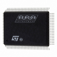
ST92F150CV1QB STMicroelectronics, ST92F150CV1QB Datasheet - Page 375

ST92F150CV1QB
Manufacturer Part Number
ST92F150CV1QB
Description
MCU 8BIT 128K FLASH 100PQFP
Manufacturer
STMicroelectronics
Series
ST9r
Datasheet
1.ST92F150CV1TB.pdf
(429 pages)
Specifications of ST92F150CV1QB
Core Processor
ST9
Core Size
8/16-Bit
Speed
24MHz
Connectivity
CAN, I²C, LIN, SCI, SPI
Peripherals
DMA, LVD, POR, PWM, WDT
Number Of I /o
77
Program Memory Size
128KB (128K x 8)
Program Memory Type
FLASH
Eeprom Size
1K x 8
Ram Size
4K x 8
Voltage - Supply (vcc/vdd)
4.5 V ~ 5.5 V
Data Converters
A/D 16x10b
Oscillator Type
Internal
Operating Temperature
-40°C ~ 105°C
Package / Case
100-QFP
Processor Series
ST92F15x
Core
ST9
Data Bus Width
8 bit, 16 bit
Data Ram Size
6 KB
Interface Type
CAN, I2C, SCI, SPI
Maximum Clock Frequency
24 MHz
Number Of Programmable I/os
80
Number Of Timers
5 x 16 bit
Operating Supply Voltage
4.5 V to 5.5 V
Maximum Operating Temperature
+ 105 C
Mounting Style
SMD/SMT
Development Tools By Supplier
ST92F150-EPB
Minimum Operating Temperature
- 40 C
On-chip Adc
16 bit x 10 bit
Lead Free Status / RoHS Status
Lead free / RoHS Compliant
Other names
497-4882
Available stocks
Company
Part Number
Manufacturer
Quantity
Price
Company:
Part Number:
ST92F150CV1QB
Manufacturer:
STMicroelectronics
Quantity:
10 000
- Current page: 375 of 429
- Download datasheet (8Mb)
11 ELECTRICAL CHARACTERISTICS
This product contains devices to protect the inputs
against damage due to high static voltages, how-
ever it is advisable to take normal precautions to
avoid application of any voltage higher than the
specified maximum rated voltages.
For proper operation it is recommended that V
and V
Reliability is enhanced if unused inputs are con-
nected to an appropriate logic voltage level (V
or V
ABSOLUTE MAXIMUM RATINGS
Notes:
Stresses above those listed as “absolute maximum ratings“ may cause permanent damage to the device. This is a stress rating only and
functional operation of the device at these conditions is not implied. Exposure to maximum rating conditions for extended periods may affect
device reliability. All voltages are referenced to V
Note 1: Pin injection current occurs when the voltage on any pin exceeds the specified range.
Note 2: Value guaranteed by design.
THERMAL CHARACTERISTICS
Symbol
SS
⎥I
V
Symbol
AV
AV
T
⎥I
V
V
⎥I
RthJA
V
INOD
TINJ
O
STG
).
INJ
AIN
DD
IO
IN
DD
SS
be higher than V
⎥
⎥
⎥
Supply Voltage
ADC Reference Voltage
ADC Ground
Input Voltage (all pins except pure open drain I/O pins)
Input Voltage (pure open drain I/O pins)
Analog Input Voltage (ADC inputs)
Storage Temperature
Load Current
Pin Injection Current - Digital and Analog Inputs
Absolute sum of all Pin Injection Current in the device
SS
PQFP100
LQFP100
and lower than V
Package
LQFP64
ST92F124/F150/F250 - ELECTRICAL CHARACTERISTICS
SS
Parameter
= 0 V.
DD
DD
IN
.
Power Considerations. The average chip-junc-
tion temperature, T
from:
Where: T
(1)
T
RthJA = Package thermal resistance
P
P
P
J
A
D
INT
PORT
=
=
Value
=
47
28
44
=
= Port power dissipation
(junction-to ambient).
(determined by the user)
T
Ambient Temperature.
P
I
DD
A
INT
– 0.3 to V
-0.3 to AV
J
V
+ P
, in Celsius can be obtained
x V
SS
– 55 to +150
+ P
– 0.3 to 6.5
– 0.3 to 6.5
to V
D
100
DD
Value
10
10
V
PORT
x RthJA
SS
DD
(chip internal power).
(2)
(2)
DD
(2)
DD
+ 0.3
+ 0.3
.
+ 0.3
°C/W
Unit
Unit
375/429
mA
mA
mA
°C
V
V
V
V
V
1
Related parts for ST92F150CV1QB
Image
Part Number
Description
Manufacturer
Datasheet
Request
R

Part Number:
Description:
BOARD PROGRAM FOR ST92F150 MCU
Manufacturer:
STMicroelectronics
Datasheet:

Part Number:
Description:
BOARD EVALUATION FOR ST9 SERIES
Manufacturer:
STMicroelectronics
Datasheet:

Part Number:
Description:
BOARD EMULATOR FOR ST9 SERIES
Manufacturer:
STMicroelectronics
Datasheet:

Part Number:
Description:
MCU, MPU & DSP Development Tools ST9 Dedication Board
Manufacturer:
STMicroelectronics
Datasheet:

Part Number:
Description:
STMicroelectronics [RIPPLE-CARRY BINARY COUNTER/DIVIDERS]
Manufacturer:
STMicroelectronics
Datasheet:

Part Number:
Description:
STMicroelectronics [LIQUID-CRYSTAL DISPLAY DRIVERS]
Manufacturer:
STMicroelectronics
Datasheet:

Part Number:
Description:
BOARD EVAL FOR MEMS SENSORS
Manufacturer:
STMicroelectronics
Datasheet:

Part Number:
Description:
NPN TRANSISTOR POWER MODULE
Manufacturer:
STMicroelectronics
Datasheet:

Part Number:
Description:
TURBOSWITCH ULTRA-FAST HIGH VOLTAGE DIODE
Manufacturer:
STMicroelectronics
Datasheet:

Part Number:
Description:
Manufacturer:
STMicroelectronics
Datasheet:

Part Number:
Description:
DIODE / SCR MODULE
Manufacturer:
STMicroelectronics
Datasheet:

Part Number:
Description:
DIODE / SCR MODULE
Manufacturer:
STMicroelectronics
Datasheet:


