DF2437FV Renesas Electronics America, DF2437FV Datasheet - Page 624
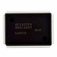
DF2437FV
Manufacturer Part Number
DF2437FV
Description
IC H8S/2437 MCU FLASH 128QFP
Manufacturer
Renesas Electronics America
Series
H8® H8S/2400r
Specifications of DF2437FV
Core Processor
H8S/2600
Core Size
16-Bit
Speed
20MHz
Connectivity
I²C, SCI
Peripherals
POR, PWM, WDT
Number Of I /o
85
Program Memory Size
256KB (256K x 8)
Program Memory Type
FLASH
Ram Size
16K x 8
Voltage - Supply (vcc/vdd)
3 V ~ 3.6 V
Data Converters
A/D 16x10b
Oscillator Type
Internal
Operating Temperature
-20°C ~ 75°C
Package / Case
128-QFP
Lead Free Status / RoHS Status
Lead free / RoHS Compliant
Eeprom Size
-
Available stocks
Company
Part Number
Manufacturer
Quantity
Price
Company:

Part Number:
DF2437FV
Manufacturer:
Renesas Electronics America
Quantity:
10 000


• R0L is a return value of FPFR.
• Since the stack area is used in the initialization program, 128-byte stack area at the maximum
• Interrupts can be accepted during the execution of the initialization program. The program
8. Check the return value in the initialization program, FPFR (general register R0L)
9. Disable all interrupts and the use of a bus master other than the CPU
10. Set FKEY to H'5A to enable the user MAT programming.
11. Set the parameter which is required for programming
• Example of the FMPAR setting
• Example of the FMPDR setting
Rev.2.00 May. 28, 2009 Page 584 of 732
REJ09B0059-0200
must be saved in RAM.
storage area and stack area in the on-chip RAM and register values must not be destroyed.
The specified voltage is applied for the specified time when programming or erasing. If
interrupts occur or the bus mastership is moved to other than the CPU during this time and the
voltage is applied for more than the specified time, flash memory may be damaged. Therefore,
interrupts and bus mastership moved to other than the CPU must be disabled.
When interrupts are disabled, bit 7 (I) in the condition code register (CCR) of the CPU should
be set to B'1 in interrupt control mode 0 or bits 7 and 6 (I and UI) in CCR should be set to B′11
in interrupt control mode 2. Then interrupts other than the NMI are retained and are not
executed.
The NMI interrupt must be masked within the user system.
The interrupts that are retained must be executed after all program processing.
The start address of the programming destination of the user MAT (FMPAR) is set to the
general register ER1. The start address of the program data area (FMPDR) is set to the general
register ER0.
FMPAR specifies the programming destination address. When an address other than one in the
user MAT area is specified, even if the programming program is executed, programming is not
executed and an error is returned to the return value parameter FPFR. Since the unit is 128
bytes, the lower eight bits of the address must be H'00 or H'80 as the boundary of 128 bytes.
When the storage destination of program data is flash memory, even if the program execution
routine is executed, programming is not executed and an error is returned to FPFR. In this
case, the program data must be transferred to the on-chip RAM and then programming must be
executed.
Related parts for DF2437FV
Image
Part Number
Description
Manufacturer
Datasheet
Request
R

Part Number:
Description:
KIT STARTER FOR M16C/29
Manufacturer:
Renesas Electronics America
Datasheet:

Part Number:
Description:
KIT STARTER FOR R8C/2D
Manufacturer:
Renesas Electronics America
Datasheet:

Part Number:
Description:
R0K33062P STARTER KIT
Manufacturer:
Renesas Electronics America
Datasheet:

Part Number:
Description:
KIT STARTER FOR R8C/23 E8A
Manufacturer:
Renesas Electronics America
Datasheet:

Part Number:
Description:
KIT STARTER FOR R8C/25
Manufacturer:
Renesas Electronics America
Datasheet:

Part Number:
Description:
KIT STARTER H8S2456 SHARPE DSPLY
Manufacturer:
Renesas Electronics America
Datasheet:

Part Number:
Description:
KIT STARTER FOR R8C38C
Manufacturer:
Renesas Electronics America
Datasheet:

Part Number:
Description:
KIT STARTER FOR R8C35C
Manufacturer:
Renesas Electronics America
Datasheet:

Part Number:
Description:
KIT STARTER FOR R8CL3AC+LCD APPS
Manufacturer:
Renesas Electronics America
Datasheet:
Part Number:
Description:
KIT STARTER FOR RX610
Manufacturer:
Renesas Electronics America
Datasheet:

Part Number:
Description:
KIT STARTER FOR R32C/118
Manufacturer:
Renesas Electronics America
Datasheet:

Part Number:
Description:
KIT DEV RSK-R8C/26-29
Manufacturer:
Renesas Electronics America
Datasheet:

Part Number:
Description:
KIT STARTER FOR SH7124
Manufacturer:
Renesas Electronics America
Datasheet:

Part Number:
Description:
KIT STARTER FOR H8SX/1622
Manufacturer:
Renesas Electronics America
Datasheet:

Part Number:
Description:
KIT DEV FOR SH7203
Manufacturer:
Renesas Electronics America
Datasheet: