DF2437FV Renesas Electronics America, DF2437FV Datasheet - Page 254
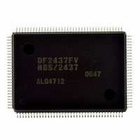
DF2437FV
Manufacturer Part Number
DF2437FV
Description
IC H8S/2437 MCU FLASH 128QFP
Manufacturer
Renesas Electronics America
Series
H8® H8S/2400r
Specifications of DF2437FV
Core Processor
H8S/2600
Core Size
16-Bit
Speed
20MHz
Connectivity
I²C, SCI
Peripherals
POR, PWM, WDT
Number Of I /o
85
Program Memory Size
256KB (256K x 8)
Program Memory Type
FLASH
Ram Size
16K x 8
Voltage - Supply (vcc/vdd)
3 V ~ 3.6 V
Data Converters
A/D 16x10b
Oscillator Type
Internal
Operating Temperature
-20°C ~ 75°C
Package / Case
128-QFP
Lead Free Status / RoHS Status
Lead free / RoHS Compliant
Eeprom Size
-
Available stocks
Company
Part Number
Manufacturer
Quantity
Price
Company:

Part Number:
DF2437FV
Manufacturer:
Renesas Electronics America
Quantity:
10 000


• PB2/FTID_1/CSYNCI_1
• PB1/TMO1_0/HSYNCO
• PB0/FTOA_0/VSYNCO
Rev.2.00 May. 28, 2009 Page 214 of 732
REJ09B0059-0200
PB2DDR
Pin function
HOE
OS3 to OS0
PB1DDR
Pin function
VOE
OEA
PB0DDR
Pin function
According to the setting of the PB2DDR bit, the pin function is switched as shown below.
When the ICIDE bit in TIER of the FRT_1 is set to 1, this pin functions as the FTID_1 input
pin. When the SIMOD1 and SIMOD0 bits (IHI signal) in TCONRI of the timer connection_1
are set to 01, this pin functions as the CSYNCI_1 input pin.
According to the combination of the HOE bit in TCONRO of the timer connection_0, the OS3
to OS0 bits in TCSR of the TMR1_0, and the PB1DDR bit, the pin function is switched as
shown below.
According to the combination of the VOE bit in TCONRO of the timer connection_0, the OEA
bit in TOCR of the FRT_0, and the PB0DDR bit, the pin function is switched as shown below.
PB0 input pin
PB1 input pin
0
0
0
All 0
PB0 output pin
PB1 output pin
PB2 input pin
1
0
0
0
1
CSYNCI_1 input pin
FTOA_0 output pin VSYNCO output pin
FTID_1 input pin
TMO1_0 output pin HSYNCO output
At least one bit is
⎯
1
set to 1
⎯
PB2 output pin
1
⎯
⎯
1
pin
⎯
⎯
1
Related parts for DF2437FV
Image
Part Number
Description
Manufacturer
Datasheet
Request
R

Part Number:
Description:
KIT STARTER FOR M16C/29
Manufacturer:
Renesas Electronics America
Datasheet:

Part Number:
Description:
KIT STARTER FOR R8C/2D
Manufacturer:
Renesas Electronics America
Datasheet:

Part Number:
Description:
R0K33062P STARTER KIT
Manufacturer:
Renesas Electronics America
Datasheet:

Part Number:
Description:
KIT STARTER FOR R8C/23 E8A
Manufacturer:
Renesas Electronics America
Datasheet:

Part Number:
Description:
KIT STARTER FOR R8C/25
Manufacturer:
Renesas Electronics America
Datasheet:

Part Number:
Description:
KIT STARTER H8S2456 SHARPE DSPLY
Manufacturer:
Renesas Electronics America
Datasheet:

Part Number:
Description:
KIT STARTER FOR R8C38C
Manufacturer:
Renesas Electronics America
Datasheet:

Part Number:
Description:
KIT STARTER FOR R8C35C
Manufacturer:
Renesas Electronics America
Datasheet:

Part Number:
Description:
KIT STARTER FOR R8CL3AC+LCD APPS
Manufacturer:
Renesas Electronics America
Datasheet:
Part Number:
Description:
KIT STARTER FOR RX610
Manufacturer:
Renesas Electronics America
Datasheet:

Part Number:
Description:
KIT STARTER FOR R32C/118
Manufacturer:
Renesas Electronics America
Datasheet:

Part Number:
Description:
KIT DEV RSK-R8C/26-29
Manufacturer:
Renesas Electronics America
Datasheet:

Part Number:
Description:
KIT STARTER FOR SH7124
Manufacturer:
Renesas Electronics America
Datasheet:

Part Number:
Description:
KIT STARTER FOR H8SX/1622
Manufacturer:
Renesas Electronics America
Datasheet:

Part Number:
Description:
KIT DEV FOR SH7203
Manufacturer:
Renesas Electronics America
Datasheet: