DF2437FV Renesas Electronics America, DF2437FV Datasheet - Page 435
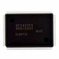
DF2437FV
Manufacturer Part Number
DF2437FV
Description
IC H8S/2437 MCU FLASH 128QFP
Manufacturer
Renesas Electronics America
Series
H8® H8S/2400r
Specifications of DF2437FV
Core Processor
H8S/2600
Core Size
16-Bit
Speed
20MHz
Connectivity
I²C, SCI
Peripherals
POR, PWM, WDT
Number Of I /o
85
Program Memory Size
256KB (256K x 8)
Program Memory Type
FLASH
Ram Size
16K x 8
Voltage - Supply (vcc/vdd)
3 V ~ 3.6 V
Data Converters
A/D 16x10b
Oscillator Type
Internal
Operating Temperature
-20°C ~ 75°C
Package / Case
128-QFP
Lead Free Status / RoHS Status
Lead free / RoHS Compliant
Eeprom Size
-
Available stocks
Company
Part Number
Manufacturer
Quantity
Price
Company:

Part Number:
DF2437FV
Manufacturer:
Renesas Electronics America
Quantity:
10 000


Notes: 1. Only 0 can be written, to clear the flag.
13.3.5
TECR selects the HSYNCO and VSYNCO output signals and the count clock source for the
TMR0 and TMR1.
Bit
0
Bit
7
6
5
4
3
2
1
0
2. The initial value is undefined since it depends on the pin state.
Bit Name
IVI
Bit Name
VS0
HS2
HS1
HS0
ICKS1_1
ICKS0_1
ICKS1_0
ICKS0_0
Timer Extended Control Register (TECR)
Initial Value
0
0
0
0
0
0
0
0
Initial Value
⎯*
2
R/W
R
R/W
R/W
R/W
R/W
R/W
R/W
R/W
R/W
R/W
Description
Vertical Synchronization Signal Output Selection
Selects the signal output from the VSYNCO with the
setting of the VOINV bit in TCONRO. See table 13.4.
Horizontal Synchronization Signal Output Select 2 to
0
Select the signal output from the HSYNCO with the
settings of the HOINV bit in TCONRO. See table
13.3.
Internal Clock Source Select (Channel 1)
Select the clock input to the timer counter (TCNT) for
the TMR0_1 and TMR1_1 and count condition with
the settings of the CKS2 to CKS0 bits in the timer
control register 1 (TCR_1). For details, see section
11.3.4, Timer Control Register (TCR).
Internal Clock Source Select (Channel 0)
Select the clock input to the timer counter (TCNT) for
the TMR0_0 and TMR1_0 and count condition with
the settings of the CKS2 to CKS0 bits in the timer
control register 0 (TCR_0). For details, see section
11.3.4, Timer Control Register (TCR).
Description
IVI Signal Level
Indicates the current level of the IVI signal. A signal
source and phase inversion are selected for the IVI
signal depends on the contents of TCONRI. Read
this bit to determine whether the input signal is
positive or negative, then hold the IVI signal at
positive phase by modifying TCONRI.
0: The IVI signal is low
1: The IVI signal is high
Rev.2.00 May. 28, 2009 Page 395 of 732
REJ09B0059-0200
Related parts for DF2437FV
Image
Part Number
Description
Manufacturer
Datasheet
Request
R

Part Number:
Description:
KIT STARTER FOR M16C/29
Manufacturer:
Renesas Electronics America
Datasheet:

Part Number:
Description:
KIT STARTER FOR R8C/2D
Manufacturer:
Renesas Electronics America
Datasheet:

Part Number:
Description:
R0K33062P STARTER KIT
Manufacturer:
Renesas Electronics America
Datasheet:

Part Number:
Description:
KIT STARTER FOR R8C/23 E8A
Manufacturer:
Renesas Electronics America
Datasheet:

Part Number:
Description:
KIT STARTER FOR R8C/25
Manufacturer:
Renesas Electronics America
Datasheet:

Part Number:
Description:
KIT STARTER H8S2456 SHARPE DSPLY
Manufacturer:
Renesas Electronics America
Datasheet:

Part Number:
Description:
KIT STARTER FOR R8C38C
Manufacturer:
Renesas Electronics America
Datasheet:

Part Number:
Description:
KIT STARTER FOR R8C35C
Manufacturer:
Renesas Electronics America
Datasheet:

Part Number:
Description:
KIT STARTER FOR R8CL3AC+LCD APPS
Manufacturer:
Renesas Electronics America
Datasheet:
Part Number:
Description:
KIT STARTER FOR RX610
Manufacturer:
Renesas Electronics America
Datasheet:

Part Number:
Description:
KIT STARTER FOR R32C/118
Manufacturer:
Renesas Electronics America
Datasheet:

Part Number:
Description:
KIT DEV RSK-R8C/26-29
Manufacturer:
Renesas Electronics America
Datasheet:

Part Number:
Description:
KIT STARTER FOR SH7124
Manufacturer:
Renesas Electronics America
Datasheet:

Part Number:
Description:
KIT STARTER FOR H8SX/1622
Manufacturer:
Renesas Electronics America
Datasheet:

Part Number:
Description:
KIT DEV FOR SH7203
Manufacturer:
Renesas Electronics America
Datasheet: