DF2437FV Renesas Electronics America, DF2437FV Datasheet - Page 36
DF2437FV
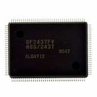
Manufacturer Part Number
DF2437FV
Description
IC H8S/2437 MCU FLASH 128QFP
Manufacturer
Renesas Electronics America
Series
H8® H8S/2400r
Specifications of DF2437FV
Core Processor
H8S/2600
Core Size
16-Bit
Speed
20MHz
Connectivity
I²C, SCI
Peripherals
POR, PWM, WDT
Number Of I /o
85
Program Memory Size
256KB (256K x 8)
Program Memory Type
FLASH
Ram Size
16K x 8
Voltage - Supply (vcc/vdd)
3 V ~ 3.6 V
Data Converters
A/D 16x10b
Oscillator Type
Internal
Operating Temperature
-20°C ~ 75°C
Package / Case
128-QFP
Lead Free Status / RoHS Status
Lead free / RoHS Compliant
Eeprom Size
-
Available stocks
Company
Part Number
Manufacturer
Quantity
Price
Company:

Part Number:
DF2437FV
Manufacturer:
Renesas Electronics America
Quantity:
10 000


Table 6.3
Table 6.4
Table 6.5
Table 6.6
Table 6.7
Table 6.8
Section 7 I/O Ports
Table 7.1
Table 7.1
Table 7.1
Table 7.1
Table 7.1
Table 7.2
Table 7.3
Table 7.4
Table 7.5
Section 8 8-Bit PWM Timer (PWM)
Table 8.1
Table 8.2
Table 8.3
Table 8.4
Table 8.5
Section 9 14-Bit PWM Timer (PWMX)
Table 9.1
Table 9.2
Table 9.3
Table 9.4
Table 9.5
Section 10 16-Bit Free-Running Timer (FRT)
Table 10.1
Table 10.2
Table 10.3
Section 11 8-Bit Timer (TMR)
Table 11.1
Table 11.2
Table 11.3
Rev.2.00 May. 28, 2009 Page xxxiv of xxxviii
REJ09B0059-0200
Bus Specifications for Normal Extended Bus Interface....................................... 100
Address Range and External Address Area (Multiplex Extended Mode)............ 101
Bus Specifications for Multiplex Extended Bus Interface (Address Cycle) ........ 101
Bus Specifications for Multiplex Extended Bus Interface (Data Cycle).............. 101
Data Buses Used and Valid Strobes..................................................................... 106
Pin States in Idle Cycle ........................................................................................ 131
Port Functions (1) ................................................................................................ 134
Port Functions (2) ................................................................................................ 135
Port Functions (3) ................................................................................................ 136
Port Functions (4) ................................................................................................ 137
Port Functions (5) ................................................................................................ 138
Port 1 Input Pull-Up MOS States......................................................................... 144
Port 2 Input Pull-Up MOS States......................................................................... 157
Port 3 Input Pull-Up MOS States......................................................................... 164
Port 6 Input Pull-Up MOS States......................................................................... 184
Pin Configuration................................................................................................. 225
Internal Clock Selection....................................................................................... 227
Resolution, PWM Conversion Period, and Carrier Frequency
when φ = 20 MHz ................................................................................................ 227
Duty Cycle of Basic Pulse ................................................................................... 230
Position of Pulses Added to Basic Pulses ............................................................ 231
Pin Configuration................................................................................................. 234
Clock Selection of PWMX .................................................................................. 239
Access Method for Reading/Writing 16-Bit Registers ........................................ 240
Settings and Operation (Examples when φ = 20 MHz)........................................ 242
Locations of Additional Pulses Added to Base Pulse (when CFS = 1)................ 246
Pin Configuration................................................................................................. 249
FRT Interrupt Sources.......................................................................................... 268
Switching of Internal Clock and FRC Operation ................................................. 273
Pin Configuration................................................................................................. 278
Clock Input to TCNT and Count Condition......................................................... 284
Interrupt Sources of 8-Bit Timers TMR0, TMR1, TMRY, and TMRX .............. 302
Related parts for DF2437FV
Image
Part Number
Description
Manufacturer
Datasheet
Request
R

Part Number:
Description:
KIT STARTER FOR M16C/29
Manufacturer:
Renesas Electronics America
Datasheet:

Part Number:
Description:
KIT STARTER FOR R8C/2D
Manufacturer:
Renesas Electronics America
Datasheet:

Part Number:
Description:
R0K33062P STARTER KIT
Manufacturer:
Renesas Electronics America
Datasheet:

Part Number:
Description:
KIT STARTER FOR R8C/23 E8A
Manufacturer:
Renesas Electronics America
Datasheet:

Part Number:
Description:
KIT STARTER FOR R8C/25
Manufacturer:
Renesas Electronics America
Datasheet:

Part Number:
Description:
KIT STARTER H8S2456 SHARPE DSPLY
Manufacturer:
Renesas Electronics America
Datasheet:

Part Number:
Description:
KIT STARTER FOR R8C38C
Manufacturer:
Renesas Electronics America
Datasheet:

Part Number:
Description:
KIT STARTER FOR R8C35C
Manufacturer:
Renesas Electronics America
Datasheet:

Part Number:
Description:
KIT STARTER FOR R8CL3AC+LCD APPS
Manufacturer:
Renesas Electronics America
Datasheet:
Part Number:
Description:
KIT STARTER FOR RX610
Manufacturer:
Renesas Electronics America
Datasheet:

Part Number:
Description:
KIT STARTER FOR R32C/118
Manufacturer:
Renesas Electronics America
Datasheet:

Part Number:
Description:
KIT DEV RSK-R8C/26-29
Manufacturer:
Renesas Electronics America
Datasheet:

Part Number:
Description:
KIT STARTER FOR SH7124
Manufacturer:
Renesas Electronics America
Datasheet:

Part Number:
Description:
KIT STARTER FOR H8SX/1622
Manufacturer:
Renesas Electronics America
Datasheet:

Part Number:
Description:
KIT DEV FOR SH7203
Manufacturer:
Renesas Electronics America
Datasheet: