DF2437FV Renesas Electronics America, DF2437FV Datasheet - Page 25
DF2437FV
Manufacturer Part Number
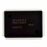
DF2437FV
Description
IC H8S/2437 MCU FLASH 128QFP
Manufacturer
Renesas Electronics America
Series
H8® H8S/2400r
Specifications of DF2437FV
Core Processor
H8S/2600
Core Size
16-Bit
Speed
20MHz
Connectivity
I²C, SCI
Peripherals
POR, PWM, WDT
Number Of I /o
85
Program Memory Size
256KB (256K x 8)
Program Memory Type
FLASH
Ram Size
16K x 8
Voltage - Supply (vcc/vdd)
3 V ~ 3.6 V
Data Converters
A/D 16x10b
Oscillator Type
Internal
Operating Temperature
-20°C ~ 75°C
Package / Case
128-QFP
Lead Free Status / RoHS Status
Lead free / RoHS Compliant
Eeprom Size
-
Available stocks
Company
Part Number
Manufacturer
Quantity
Price
Company:

Part Number:
DF2437FV
Manufacturer:
Renesas Electronics America
Quantity:
10 000


Section 1 Overview
Figure 1.1
Figure 1.2
Figure 1.3
Section 2 CPU
Figure 2.1
Figure 2.2
Figure 2.3
Figure 2.4
Figure 2.5
Figure 2.6
Figure 2.7
Figure 2.8
Figure 2.9
Figure 2.9
Figure 2.10
Figure 2.11
Figure 2.12
Figure 2.13
Section 3 MCU Operating Modes
Figure 3.1
Section 4 Exception Handling
Figure 4.1
Figure 4.2
Figure 4.3
Section 5 Interrupt Controller
Figure 5.1
Figure 5.2
Figure 5.3
Figure 5.4
Figure 5.5
Figure 5.6
Section 6 Bus Controller (BSC)
Figure 6.1
Figure 6.2
Internal Block Diagram of H8S/2437 Group .......................................................2
Pin Assignment of H8S/2437 Group (FP-128B)..................................................3
Sample Design of Reset Signals without Affection Each Other ..........................14
Exception-Handling Vector Table (Normal Mode) .............................................19
Stack Structure in Normal Mode..........................................................................19
Exception-Handling Vector Table (Advanced Mode) .........................................20
Stack Structure in Advanced Mode......................................................................21
Memory Map .......................................................................................................22
CPU Registers......................................................................................................23
Usage of General Registers..................................................................................24
Stack.....................................................................................................................25
General Register Data Formats (1) ......................................................................28
General Register Data Formats (2) ......................................................................29
Memory Data Formats .........................................................................................30
Instruction Formats (Examples)...........................................................................42
Branch Address Specification in Memory Indirect Mode....................................46
State Transitions...................................................................................................50
Memory Map .......................................................................................................56
Reset Sequence ....................................................................................................60
Stack Status after Exception Handling.................................................................63
Operation when SP Value is Odd.........................................................................64
Block Diagram of Interrupts IRQ7 to IRQ0.........................................................77
Flowchart of Procedure Up to Interrupt Acceptance
Flowchart of Procedure Up to Interrupt Acceptance
Interrupt Exception Handling...............................................................................87
Contention between Interrupt Generation and Disabling.....................................90
Block Diagram of Bus Controller ........................................................................94
CSn Signal Output Polarity and Output Timing ..................................................102
Block Diagram of Interrupt Controller ................................................................66
in Interrupt Control Mode 0 .................................................................................83
in Interrupt Control Mode 2 .................................................................................85
Figures
Rev.2.00 May. 28, 2009 Page xxiii of xxxviii
REJ09B0059-0200
Related parts for DF2437FV
Image
Part Number
Description
Manufacturer
Datasheet
Request
R

Part Number:
Description:
KIT STARTER FOR M16C/29
Manufacturer:
Renesas Electronics America
Datasheet:

Part Number:
Description:
KIT STARTER FOR R8C/2D
Manufacturer:
Renesas Electronics America
Datasheet:

Part Number:
Description:
R0K33062P STARTER KIT
Manufacturer:
Renesas Electronics America
Datasheet:

Part Number:
Description:
KIT STARTER FOR R8C/23 E8A
Manufacturer:
Renesas Electronics America
Datasheet:

Part Number:
Description:
KIT STARTER FOR R8C/25
Manufacturer:
Renesas Electronics America
Datasheet:

Part Number:
Description:
KIT STARTER H8S2456 SHARPE DSPLY
Manufacturer:
Renesas Electronics America
Datasheet:

Part Number:
Description:
KIT STARTER FOR R8C38C
Manufacturer:
Renesas Electronics America
Datasheet:

Part Number:
Description:
KIT STARTER FOR R8C35C
Manufacturer:
Renesas Electronics America
Datasheet:

Part Number:
Description:
KIT STARTER FOR R8CL3AC+LCD APPS
Manufacturer:
Renesas Electronics America
Datasheet:
Part Number:
Description:
KIT STARTER FOR RX610
Manufacturer:
Renesas Electronics America
Datasheet:

Part Number:
Description:
KIT STARTER FOR R32C/118
Manufacturer:
Renesas Electronics America
Datasheet:

Part Number:
Description:
KIT DEV RSK-R8C/26-29
Manufacturer:
Renesas Electronics America
Datasheet:

Part Number:
Description:
KIT STARTER FOR SH7124
Manufacturer:
Renesas Electronics America
Datasheet:

Part Number:
Description:
KIT STARTER FOR H8SX/1622
Manufacturer:
Renesas Electronics America
Datasheet:

Part Number:
Description:
KIT DEV FOR SH7203
Manufacturer:
Renesas Electronics America
Datasheet: