DF2437FV Renesas Electronics America, DF2437FV Datasheet - Page 32
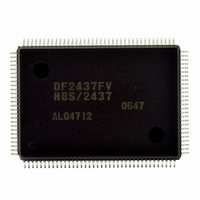
DF2437FV
Manufacturer Part Number
DF2437FV
Description
IC H8S/2437 MCU FLASH 128QFP
Manufacturer
Renesas Electronics America
Series
H8® H8S/2400r
Specifications of DF2437FV
Core Processor
H8S/2600
Core Size
16-Bit
Speed
20MHz
Connectivity
I²C, SCI
Peripherals
POR, PWM, WDT
Number Of I /o
85
Program Memory Size
256KB (256K x 8)
Program Memory Type
FLASH
Ram Size
16K x 8
Voltage - Supply (vcc/vdd)
3 V ~ 3.6 V
Data Converters
A/D 16x10b
Oscillator Type
Internal
Operating Temperature
-20°C ~ 75°C
Package / Case
128-QFP
Lead Free Status / RoHS Status
Lead free / RoHS Compliant
Eeprom Size
-
Available stocks
Company
Part Number
Manufacturer
Quantity
Price
Company:

Part Number:
DF2437FV
Manufacturer:
Renesas Electronics America
Quantity:
10 000


Figure 20.4
Figure 20.5
Figure 20.6
Figure 20.7
Figure 20.8
Figure 20.9
Figure 20.10 RAM Map when Programming/Erasing is Executed........................................... 580
Figure 20.11 Programming Procedure ...................................................................................... 581
Figure 20.12 Erasing Procedure ................................................................................................ 586
Figure 20.13 Repeating Procedure of Erasing and Programming ............................................. 588
Figure 20.14 Procedure for Programming User MAT in User Boot Mode............................... 590
Figure 20.15 Procedure for Erasing User MAT in User Boot Mode......................................... 592
Figure 20.16 Transitions to Error Protection State.................................................................... 605
Figure 20.17 Switching between User MAT and User Boot MAT........................................... 606
Figure 20.18 Memory Map in Programmer Mode .................................................................... 607
Figure 20.19 Boot Program States ............................................................................................ 609
Figure 20.20 Bit-Rate-Adjustment Sequence............................................................................ 610
Figure 20.21 Communication Protocol Format......................................................................... 611
Figure 20.22 New Bit-Rate Selection Sequence ....................................................................... 622
Figure 20.23 Programming Sequence ....................................................................................... 625
Figure 20.24 Erasure Sequence................................................................................................. 628
Section 21 Clock Pulse Generator
Figure 21.1
Figure 21.2
Figure 21.3
Figure 21.4
Figure 21.5
Figure 21.6
Figure 21.7 Note on Board Design of Oscillation Circuit Section.............................................. 644
Section 22 Power-Down Modes
Figure 22.1
Figure 22.2
Figure 22.3
Section 24 Electrical Characteristics
Figure 24.1
Figure 24.2
Figure 24.3
Figure 24.4
Figure 24.5
Figure 24.6
Figure 24.7
Rev.2.00 May. 28, 2009 Page xxx of xxxviii
REJ09B0059-0200
Block Division of User MAT............................................................................... 554
Overview of User Procedure Program ................................................................. 555
System Configuration in Boot Mode ................................................................... 576
Automatic-Bit-Rate Adjustment Operation of SCI.............................................. 576
Overview of State Transition Diagram in Boot Mode ......................................... 578
Overview of Programming/Erasing Flow ............................................................ 579
Block Diagram of Clock Pulse Generator............................................................ 637
Typical Connection to Crystal Resonator ............................................................ 640
Equivalent Circuit of Crystal Resonator .............................................................. 640
Example of External Clock Input......................................................................... 641
External Clock Input Timing ............................................................................... 642
Timing of Output Stabilization Delay Time for External Clock.......................... 643
Mode Transitions ................................................................................................. 647
Software Standby Mode Application Example.................................................... 655
Hardware Standby Mode Timing......................................................................... 657
Darlington Transistor Drive Circuit (Example) ................................................... 701
Output Load Circuit ............................................................................................. 701
System Clock Timing .......................................................................................... 702
Oscillation Stabilization Timing .......................................................................... 703
Oscillation Stabilization Timing (Exiting Software Standby Mode) ................... 703
Reset Input Timing .............................................................................................. 704
Interrupt Input Timing ......................................................................................... 705
Related parts for DF2437FV
Image
Part Number
Description
Manufacturer
Datasheet
Request
R

Part Number:
Description:
KIT STARTER FOR M16C/29
Manufacturer:
Renesas Electronics America
Datasheet:

Part Number:
Description:
KIT STARTER FOR R8C/2D
Manufacturer:
Renesas Electronics America
Datasheet:

Part Number:
Description:
R0K33062P STARTER KIT
Manufacturer:
Renesas Electronics America
Datasheet:

Part Number:
Description:
KIT STARTER FOR R8C/23 E8A
Manufacturer:
Renesas Electronics America
Datasheet:

Part Number:
Description:
KIT STARTER FOR R8C/25
Manufacturer:
Renesas Electronics America
Datasheet:

Part Number:
Description:
KIT STARTER H8S2456 SHARPE DSPLY
Manufacturer:
Renesas Electronics America
Datasheet:

Part Number:
Description:
KIT STARTER FOR R8C38C
Manufacturer:
Renesas Electronics America
Datasheet:

Part Number:
Description:
KIT STARTER FOR R8C35C
Manufacturer:
Renesas Electronics America
Datasheet:

Part Number:
Description:
KIT STARTER FOR R8CL3AC+LCD APPS
Manufacturer:
Renesas Electronics America
Datasheet:
Part Number:
Description:
KIT STARTER FOR RX610
Manufacturer:
Renesas Electronics America
Datasheet:

Part Number:
Description:
KIT STARTER FOR R32C/118
Manufacturer:
Renesas Electronics America
Datasheet:

Part Number:
Description:
KIT DEV RSK-R8C/26-29
Manufacturer:
Renesas Electronics America
Datasheet:

Part Number:
Description:
KIT STARTER FOR SH7124
Manufacturer:
Renesas Electronics America
Datasheet:

Part Number:
Description:
KIT STARTER FOR H8SX/1622
Manufacturer:
Renesas Electronics America
Datasheet:

Part Number:
Description:
KIT DEV FOR SH7203
Manufacturer:
Renesas Electronics America
Datasheet: