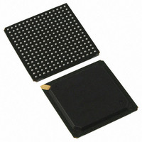
PI7C9X130DNDE Pericom Semiconductor, PI7C9X130DNDE Datasheet - Page 40

PI7C9X130DNDE
Manufacturer Part Number
PI7C9X130DNDE
Description
IC PCIE-PCIX BRIDGE 1PORT 256BGA
Manufacturer
Pericom Semiconductor
Specifications of PI7C9X130DNDE
Applications
PCI-to-PCI Bridge
Interface
SMBus (2-Wire/I²C)
Voltage - Supply
1.8V, 3.3V
Package / Case
256-PBGA
Mounting Type
Surface Mount
Operating Temperature (min)
-40C
Operating Temperature Classification
Industrial
Operating Temperature (max)
85C
Package Type
BGA
Rad Hardened
No
Lead Free Status / RoHS Status
Lead free / RoHS Compliant
Available stocks
Company
Part Number
Manufacturer
Quantity
Price
Company:
Part Number:
PI7C9X130DNDE
Manufacturer:
Pericom
Quantity:
135
Company:
Part Number:
PI7C9X130DNDE
Manufacturer:
NSC
Quantity:
70
7.4.4 PRIMARY STATUS REGISTER – OFFSET 04h
PERICOM SEMICONDUCTOR - Confidential
Bit
3
4
5
6
7
8
9
10
15:11
Bit
19:16
20
21
22
Function
Special Cycle
Enable
Memory Write and
Invalidate Enable
VGA Palette Snoop
Enable
Parity Error
Response Enable
Wait Cycle Control
SERR_L Enable Bit
Fast Back-to-Back
Enable
Interrupt Disable
Reserved
Function
Reserved
Capability List
Capable
66MHz Capable
Reserved
RO / RW
RO / RW
Type
Type
RW
RW
RO
RO
RO
RO
RO
RO
RO
RO
RO
Page 40 of 165
Description
0: PI7C9X130 does not respond as a target to Special Cycle transactions, so
this bit is defined as Read-Only and must return 0 when read
Reset to 0
0: PI7C9X130 does not originate a Memory Write and Invalidate transaction.
Implements this bit as Read-Only and returns 0 when read (unless forwarding a
transaction for another master). This bit will be ignored in PCI-X mode.
Reset to 0
This bit applies to reverse bridge only.
0: Ignore VGA palette access on the primary
1: Enable positive decoding response to VGA palette writes on the primary
interface with I/O address bits AD [9:0] equal to 3C6h, 3C8h, and 3C9h
(inclusive of ISA alias; AD [15:0] are not decoded and may be any value)
Reset to 0
0: May ignore any parity error that is detected and take its normal action
1: This bit if set, enables the setting of Master Data Parity Error bit in the
Status Register when poisoned TLP received or parity error is detected and
takes its normal action
Reset to 0
Wait cycle control not supported
Reset to 0
0: Disable
1: Enable PI7C9X130 in forward bridge mode to report non-fatal or fatal
error message to the Root Complex. Also, in reverse bridge mode to assert
SERR_L on the primary interface
Reset to 0
Fast back-to-back enable not supported
Reset to 0
This bit applies to reverse bridge only.
0: INTA_L, INTB_L, INTC_L, and INTD_L can be asserted on PCI interface
1: Prevent INTA_L, INTB_L, INTC_L, and INTD_L from being asserted on
PCI interface
Reset to 0
Reset to 00000
Description
Reset to 0000
1: PI7C9X130 supports the capability list (offset 34h in the pointer to the data
structure)
Reset to 1
This bit applies to reverse bridge only.
1: 66MHz capable
Reset to 0 when forward bridge or 1 when reverse bridge.
Reset to 0
PCI EXPRESS TO PCI-X BRIDGE
Mar 2010 - Rev 2.0
PI7C9X130


