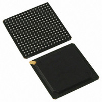
PI7C9X130DNDE Pericom Semiconductor, PI7C9X130DNDE Datasheet - Page 28

PI7C9X130DNDE
Manufacturer Part Number
PI7C9X130DNDE
Description
IC PCIE-PCIX BRIDGE 1PORT 256BGA
Manufacturer
Pericom Semiconductor
Specifications of PI7C9X130DNDE
Applications
PCI-to-PCI Bridge
Interface
SMBus (2-Wire/I²C)
Voltage - Supply
1.8V, 3.3V
Package / Case
256-PBGA
Mounting Type
Surface Mount
Operating Temperature (min)
-40C
Operating Temperature Classification
Industrial
Operating Temperature (max)
85C
Package Type
BGA
Rad Hardened
No
Lead Free Status / RoHS Status
Lead free / RoHS Compliant
Available stocks
Company
Part Number
Manufacturer
Quantity
Price
Company:
Part Number:
PI7C9X130DNDE
Manufacturer:
Pericom
Quantity:
135
Company:
Part Number:
PI7C9X130DNDE
Manufacturer:
NSC
Quantity:
70
PI7C9X130
PCI EXPRESS TO PCI-X BRIDGE
secondary interface. In addition, CSRs (Control and Status Registers) are implemented to support the
memory or IO transfers between the primary and secondary buses. The CSRs are accessed through
memory transaction access within the lowest memory range of 4K Space (bit [64:12] are zeros). The
non-transparent configuration registers can be accessed through several different ways (PCI Express, PCI,
I2C, and SM bus). For PCI Express and PCI access, the type-0 configuration transactions need to be
used. For I2C access, I2C bus protocol needs to be used through I2C bus interface. For SM bus
access, SM bus protocol needs to be used through SM bus interface. The hardware pins (B5 and A5)
are shared for I2C and SM bus interface. If TM1=0, pins B5 and A5 will be SCL and SDA for I2C
interface respectively. If TM1=1, pins B5 and A5 will be SMBCLK and SMBDAT for SM Bus
interface respectively.
In non-transparent bridge mode, PI7C9X130 supports four or three memory BARs (Base Address
Registers) and one or two IO BARs (Base Address Registers) depending on selection on the primary bus.
Also, PI7C9X130 supports four or three memory BARs (Base Address Registers) and one or two IO
BARs (Base Address Registers) depending on selection on the secondary bus.
Offset 10h is defined to be primary CSR and downstream memory 0 BAR. Offset 14h is defined to be
primary CSR and downstream IO BAR. Offset 18h is defined to be downstream memory 1 or IO BAR
(selectable by CSR setup register). Offset 1Ch is defined to be downstream memory 2 BAR. Offset
20h and 24h are defined to be downstream memory 3 lower BAR and memory 3 upper BAR respectively
to support 64-bit decoding.
The direct offset translation of address from primary to secondary bus will be done by substituting the
original Base Address at primary with the downstream Translation Base Address Register values and
keeping the lower address bits the same to form a new address for forward the transaction to secondary
bus.
For downstream memory 2, it uses direct address translation. There is no lookup table for downstream
memory address translation.
Offset 50h is defined to be secondary CSR and upstream memory 0 BAR. Offset 54h is defined to be
secondary CSR and upstream IO BAR. Offset 58h is defined to be upstream memory 1 or IO BAR
(selectable by CSR setup register offset E4h). Offset 1Ch is defined to be upstream memory 2 BAR.
Offset 60h and 64h are defined to be upstream memory 3 lower BAR and memory 3 upper BAR
respectively to support 64-bit decoding.
The direct offset translation of address from secondary to primary bus will be done by substituting the
original Base Address at secondary with the upstream Translation Base Address Register values and
keeping the lower address bits the same to form a new address for forward the transaction to primary bus.
For upstream memory 2, it uses lookup table address translation method which using the original base
address as index to select a new address on the upstream memory 2 lookup table based on the page and
window size defined.
Page 28 of 165
PERICOM SEMICONDUCTOR - Confidential
Mar 2010 - Rev 2.0


