PI7C9X130DNDE Pericom Semiconductor, PI7C9X130DNDE Datasheet
PI7C9X130DNDE
Specifications of PI7C9X130DNDE
Available stocks


Related parts for PI7C9X130DNDE

PI7C9X130DNDE Summary of contents
Page 1
PI7C9X130 PCI Express to PCI-X Reversible Bridge 3545 North First Street, San Jose, CA 95134 Telephone: 1-877-PERICOM, (1-877-737-4266) Fax: 408-435-1100 Internet: http://www.pericom.com Revision 2.0 ...
Page 2
... A critical component is any component of a life support device or system whose failure to perform can be reasonably expected to cause the failure of the life support device or system affect its safety or effectiveness. Pericom Semiconductor Corporation reserves the right to make changes to its products or specifications at any time, without notice, in order to improve design or performance and to supply the best possible product ...
Page 3
... PREFACE PERICOM SEMICONDUCTOR - Confidential Description First Draft of PI7C9X130 Data Sheet Correct INTA buffer type Update configuration map and registers Update JTAG chain order Add PCI/PCI-X selection information Update on configuration register bit definitions. 1) Bit [10, 7:2] of offset 40h ...
Page 4
... The datasheet of PI7C9X130 will be enhanced periodically when updated information is available. in this datasheet is subject to change without notice. Bridge) and provides technical information for designers to design their hardware using PI7C9X130. PERICOM SEMICONDUCTOR - Confidential PCI EXPRESS TO PCI-X BRIDGE This document describes the functionalities of PI7C9X130 (PCI Express ...
Page 5
... This page intentionally left blank. PERICOM SEMICONDUCTOR - Confidential PCI EXPRESS TO PCI-X BRIDGE Page 5 of 165 PI7C9X130 Mar 2010 - Rev 2.0 ...
Page 6
... SUBORDINATE BUS NUMBER REGISTER – OFFSET 18h .............................................................43 7.4.14 SECONDARY LATENCY TIMER REGISTER – OFFSET 18h............................................................43 7.4.15 I/O BASE REGISTER – OFFSET 1Ch.................................................................................................43 7.4.16 I/O LIMIT REGISTER – OFFSET 1Ch................................................................................................44 PERICOM SEMICONDUCTOR - Confidential PCI EXPRESS TO PCI-X BRIDGE Page 6 of 165 PI7C9X130 Mar 2010 - Rev 2.0 ...
Page 7
... PCI EXPRESS CAPABILITY ID REGISTER – OFFSET B0h .............................................................63 7.4.68 NEXT CAPABILITY POINTER REGISTER – OFFSET B0h...............................................................64 7.4.69 PCI EXPRESS CAPABILITY REGISTER – OFFSET B0h ..................................................................64 7.4.70 DEVICE CAPABILITY REGISTER – OFFSET B4h............................................................................64 PERICOM SEMICONDUCTOR - Confidential PCI EXPRESS TO PCI-X BRIDGE Page 7 of 165 PI7C9X130 Mar 2010 - Rev 2.0 ...
Page 8
... PORT VC STATUS REGISTER – OFFSET 15Ch............................................................................80 7.4.122 VC0 RESOURCE CAPBILITY REGISTER – OFFSET 160h...........................................................81 7.4.123 VC0 RESOURCE CONTROL REGISTER – OFFSET 164h ............................................................81 7.4.124 VC0 RESOURCE STATUS REGISTER – OFFSET 168h ................................................................81 PERICOM SEMICONDUCTOR - Confidential PCI EXPRESS TO PCI-X BRIDGE Page 8 of 165 PI7C9X130 Mar 2010 - Rev 2.0 ...
Page 9
... SUBSYSTEM ID REGISTER – OFFSET 6Ch....................................................................................103 7.5.45 EEPROM AUTOLOAD CONTROL/STATUS REGISTER – OFFSET 70h........................................103 7.5.46 HOT SWAP CONTROL AND STATUS REGISTER – OFFSET 74h .................................................104 PERICOM SEMICONDUCTOR - Confidential PCI EXPRESS TO PCI-X BRIDGE Page 9 of 165 PI7C9X130 Mar 2010 - Rev 2.0 ...
Page 10
... NEXT CAPABILITY POINTER REGISTER – OFFSET F0h.............................................................123 7.5.98 MESSAGE CONTROL REGISTER – OFFSET F0h ..........................................................................123 7.5.99 MESSAGE ADDRESS REGISTER – OFFSET F4h ...........................................................................124 7.5.100 MESSAGE UPPER ADDRESS REGISTER – OFFSET F8h .........................................................124 PERICOM SEMICONDUCTOR - Confidential PCI EXPRESS TO PCI-X BRIDGE Page 10 of 165 PI7C9X130 Mar 2010 - Rev 2.0 ...
Page 11
... UPSTREAM PAGE BOUNDARY IRQ 0 MASK REGISTER - OFFSET 060h...................................138 7.6.16 UPSTREAM PAGE BOUNDARY IRQ 1 MASK REGISTER - OFFSET 064h...................................138 7.6.17 RESERVED REGISTER – OFFSET 068C.........................................................................................138 PERICOM SEMICONDUCTOR - Confidential PCI EXPRESS TO PCI-X BRIDGE Page 11 of 165 PI7C9X130 Mar 2010 - Rev 2.0 ...
Page 12
... ELECTRICAL AND TIMING SPECIFICATIONS ................................................................................157 16.1 ABSOLUTE MAXIMUM RATINGS .......................................................................................................157 16.2 DC SPECIFICATIONS .............................................................................................................................157 16.3 POWER-UP SEQUENCING.....................................................................................................................158 16.4 AC SPECIFICATIONS .............................................................................................................................159 17 PACKAGE INFORMATION.....................................................................................................................162 18 ORDERING INFORMATION...................................................................................................................164 PERICOM SEMICONDUCTOR - Confidential PCI EXPRESS TO PCI-X BRIDGE Page 12 of 165 PI7C9X130 Mar 2010 - Rev 2.0 ...
Page 13
... ASYNCHRONOUS CLOCK......................................................................................................................165 19.1 19.1 ASYNCHRONOUS CLOCK SUPPORT ..........................................................................................165 PERICOM SEMICONDUCTOR - Confidential PCI EXPRESS TO PCI-X BRIDGE Page 13 of 165 PI7C9X130 Mar 2010 - Rev 2.0 ...
Page 14
... F 16-18 PCI S T IGURE IGNAL IMING F 17- IGURE OP IEW RAWING F 17- IGURE OTTOM IEW RAWING F 17- IGURE ACKAGE UTLINE PERICOM SEMICONDUCTOR - Confidential R D .....................................................................................150 EGISTER EFINITION R .............................................................................................................157 ATINGS .......................................................................................................157 ...............................................................................................................159 .............................................................................................................................15 ................................................................................................................24 ..........................................................................................................................25 M .............................................................................................26 TRANSPARENT ODE M .......................................................................................................27 ODE R ..............................................................................................................29 EGISTERS M (00 – ......................................................................................31 AP ...
Page 15
... CRC (16-bit), LCRC (32-bit) ECRC and advanced error reporting PRBS (Pseudo Random Bit Sequencing) generator/checker for chip testing Maximum payload size to 512 bytes PERICOM SEMICONDUCTOR - Confidential PCI Express Link PCI-X 64-bit, 133MHz Bus Page 15 of 165 PI7C9X130 PCI EXPRESS TO PCI-X BRIDGE Mar 2010 - Rev 2 ...
Page 16
... EEPROM (I2C) Interface Industril Temp Compliant (-40˚C ~ +85˚C) SM Bus Interface Auxiliary powers (VAUX, VDDAUX, VDDCAUX) support Power consumption at about 1.5 Watt in typical condition PERICOM SEMICONDUCTOR - Confidential PCI EXPRESS TO PCI-X BRIDGE Page 16 of 165 PI7C9X130 Mar 2010 - Rev 2.0 ...
Page 17
... TBN G3 TCP J4, TCN J3 TDP L4, TDN L3 RREF H4 PERST_L P1 PERICOM SEMICONDUCTOR - Confidential Bi-directional Input Input with pull-up Input with pull-down Bi-directional with open drain output Open drain output Output Power Ground PIN TYPE Reference Clock Input s: Connect to external 100MHz differential I clock. These signals require AC coupled with 0.1uF capacitors. ...
Page 18
... CBE [7:4] P13, P15, A14, C11 PAR F14 PAR64 D15 PERICOM SEMICONDUCTOR - Confidential PIN TYPE Address / Data: Multiplexed address and data bus. Address phase is B aligned with first clock of FRAME_L assertion. Data phase is aligned with IRDY_L or TRDY_L assertion. Data is transferred on rising edges of FBCLKIN when both IRDY_L and TRDY_L are asserted ...
Page 19
... P3, N3, T2, R2, P2, R1 GNT_L [5:0] T5, R5, P5, N5, T4, R4 REQ64_L D14 PERICOM SEMICONDUCTOR - Confidential PIN TYPE FRAME (Active LOW): Driven by the initiator of a transaction to B indicate the beginning and duration an access. The de-assertion of FRAME_L indicates the final data phase signaled by the initiator in burst transfers ...
Page 20
... N14 CFN_L P7 2.5 JTAG BOUNDARY SCAN SIGNALS NAME ASSIGNMENT PERICOM SEMICONDUCTOR - Confidential PIN TYPE Acknowledge for 64-bit transfer (Active LOW): When PI7C9X130 target device and drives ACK64_L to signal the bus master to use 64- bit transfer. When PI7C9X130 is the bus master, ACK64_L is an input ...
Page 21
... HSEN R3 HSSW T3 LOO N6 ENUM_L P6 PERICOM SEMICONDUCTOR - Confidential PIN TYPE Test Clock: TCK is the test clock to synchronize the state information IU and data on the PCI bus side of PI7C9X130 during boundary scan operation. Test Mode Select: TMS controls the state of the Test Access Port IU (TAP) controller ...
Page 22
... AD[23] A9 AD[19] A10 CBE[2] A11 DEVSEL_L A12 AD[33] PERICOM SEMICONDUCTOR - Confidential PIN TYPE Analog Voltage Supply for PCI Express Interface: Connect to the P 1.8V Power Supply. Digital Voltage Supply for PCI Express Interface: Connect to the P 1.8V Power Supply. Auxiliary Voltage Supply for PCI Express Interface: Connect to the P 1 ...
Page 23
... AD[27] D7 CBE[3] D8 AD[20] D9 AD[16] D10 TRDY_L D11 AD[32] D12 AD[36] D13 VD33 D14 REQ64_L D15 PAR64 D16 AD[47] PERICOM SEMICONDUCTOR - Confidential Pin Name Pin Name E13 LOCK_L J13 AD[5] E14 SEL100 J14 AD[6] E15 DEV64 J15 AD[7] E16 ACK64_L J16 CBE[0] ...
Page 24
... If PI7C9X130 sees logic HIGH on SEL100, the secondary bus is initialized to PCI-X 100MHz mode. If the value is LOW, PCI-X 133MHz is initialized. These two clock frequencies allow the flexibility to support different bus loading conditions. PERICOM SEMICONDUCTOR - Confidential PCI EXPRESS TO PCI-X BRIDGE TM0 ...
Page 25
... Table 3-2 to show the states of operations during the PCI Express PERST_L de- assertion transition in forward bridge mode or PCI RESET_L de-assertion transition in reverse bridge mode. Figure 3-5 Pin Strapping TM2 Strapped TM1 Strapped PERICOM SEMICONDUCTOR - Confidential 3. Weak Ohms Pull-up PCIXCAP 1K Strong Ohms Pull-up 0.01uF PCIXUP PCI Card 3 ...
Page 26
... PCI Express x4 link. It enables the legacy PCI/PCI-X Host Systems to provide PCI Express capability. PI7C9X130 provides a solution to convert existing PCI/PCI-X based designs to adapt quickly into PCI Express base platforms. Existing PIC/PCI-X based applications will not have to undergo a complete re- architecture in order to interface to PCI Express technology. PERICOM SEMICONDUCTOR - Confidential Host Processor Root ...
Page 27
... PI7C9X130 has type-0 configuration header if TM0 is set to 1 (non-transparent mode). The configuration registers are similar to a traditional PCI device. However, there is one set of configuration registers for the primary interface and another set of configuration registers for the PERICOM SEMICONDUCTOR - Confidential Host Processor ...
Page 28
... For upstream memory 2, it uses lookup table address translation method which using the original base address as index to select a new address on the upstream memory 2 lookup table based on the page and window size defined. PERICOM SEMICONDUCTOR - Confidential PCI EXPRESS TO PCI-X BRIDGE Page 28 of 165 PI7C9X130 Mar 2010 - Rev 2 ...
Page 29
... Data payload of PI7C9X130 can range from 4 (1DW) to 256 (64DW) bytes. PI7C9X130 supports three TLP routing mechanisms. They are comprised of Address, ID, and Implicit routings. Address routing is being used for Memory and IO requests. ID based (bus, device, function numbers) routing is being PERICOM SEMICONDUCTOR - Confidential Typical Access Configuration access offset 10h ...
Page 30
... TC0, PI7C9X130 will treat them as malformed packets. PI7C9X130 maps all downstream memory packets from PCI Express to PCI transactions regardless the virtual isochronous operation is enabled or not. PERICOM SEMICONDUCTOR - Confidential PCI EXPRESS TO PCI-X BRIDGE PI7C9X130 accepts only TC0 packets of configuration, IO, ...
Page 31
... PERICOM SEMICONDUCTOR - Confidential PCI EXPRESS TO PCI-X BRIDGE Transparent Non- Mode (type1) Transparent Mode (Type0) Vendor ID Vendor ID Device ID ...
Page 32
... PERICOM SEMICONDUCTOR - Confidential PCI EXPRESS TO PCI-X BRIDGE Transparent Non- Mode (type1) Transparent Mode (Type0) Header Type ...
Page 33
... PERICOM SEMICONDUCTOR - Confidential PCI EXPRESS TO PCI-X BRIDGE Transparent Non- Mode (type1) Transparent Mode (Type0) Capability Capability Pointer ...
Page 34
... A3h – A0h A3h – A0h A7h – A4h A7h – A4h ABh – A8h ABh – A8h PERICOM SEMICONDUCTOR - Confidential PCI EXPRESS TO PCI-X BRIDGE Transparent Non- Mode (type1) Transparent Mode (Type0) Vendor ID ...
Page 35
... EFh – ECh F3h – F0h F3h – F0h F7h – F4h F7h – F4h FBh – F8h FBh – F8h FFh – FCh FFh – FCh PERICOM SEMICONDUCTOR - Confidential PCI EXPRESS TO PCI-X BRIDGE Transparent Non- Mode (type1) Transparent Mode (Type0) Base ...
Page 36
... PERICOM SEMICONDUCTOR - Confidential PCI EXPRESS TO PCI-X BRIDGE Transparent Non- Mode (type1) Transparent Mode (Type0) Advanced Error ...
Page 37
... PERICOM SEMICONDUCTOR - Confidential PCI EXPRESS TO PCI-X BRIDGE Transparent Non- Mode (type1) Transparent Mode (Type0) Port VC ...
Page 38
... PERICOM SEMICONDUCTOR - Confidential PCI EXPRESS TO PCI-X BRIDGE Register Reset Value Name Downstream 0000_0000h Memory 3 Upper 32-bit ...
Page 39
... Bit Function 31:16 Device ID 7.4.3 COMMAND REGISTER – OFFSET 04h Bit Function 0 I/O Space Enable 1 Memory Space Enable 2 Bus Master Enable PERICOM SEMICONDUCTOR - Confidential Register Reset Value Name Upstream 0 Memory 2 Lookup Table Reserved 0 Descriptions Read Only Read Only and Sticky Read/Write Read Only at primary interface and Read/Write at secondary interface Read/Write “ ...
Page 40
... Reserved 20 Capability List Capable 21 66MHz Capable 22 Reserved PERICOM SEMICONDUCTOR - Confidential Type Description RO 0: PI7C9X130 does not respond as a target to Special Cycle transactions, so this bit is defined as Read-Only and must return 0 when read Reset PI7C9X130 does not originate a Memory Write and Invalidate transaction. ...
Page 41
... Received Master Abort 30 Signaled System Error 31 Detected Parity Error PERICOM SEMICONDUCTOR - Confidential Type Description This bit applies to reverse bridge only Enable fast back-to-back transactions Reset to 0 when forward bridge or 1 when reverse bridge in PCI mode. RWC Bit set if its Parity Error Enable bit is set and either of the conditions occurs on the primary: FORWARD BRIDGE – ...
Page 42
... Cache Line Size 5 Cache Line Size 7:6 Reserved 7.4.8 PRIMARY LATENCY TIMER REGISTER – OFFSET 0Ch Bit Function 15:8 Primary Latency Timer PERICOM SEMICONDUCTOR - Confidential Type Description RO Reset to 00000000 Type Description RO Subtractive decoding of PCI-PCI bridge not supported Reset to 00000000 RO Sub-Class Code ...
Page 43
... Secondary Latency Timer 7.4.15 I/O BASE REGISTER – OFFSET 1Ch Bit Function 1:0 32-bit I/O Addressing Support 3:2 Reserved PERICOM SEMICONDUCTOR - Confidential Type Description RO PCI-to-PCI bridge configuration (10 – 3Fh) Reset to 0000001 RO 0: Indicates single function device Reset Reset to 00h Type ...
Page 44
... Reserved 23 Fast Back-to-Back Capable 24 Master Data Parity Error Detected 26:25 DEVSEL_L Timing (medium decoding) 27 Signaled Target Abort PERICOM SEMICONDUCTOR - Confidential Type Description RW Indicates the I/O Base (0000_0000h) Reset to 0000 Type Description RO 01: Indicates PI7C9X130 supports 32-bit I/O addressing Reset Reset to 00 ...
Page 45
... Addressing Support 15:4 Prefetchable Memory Base PERICOM SEMICONDUCTOR - Confidential RWC FORWARD BRIDGE – Bit is set when PI7C9X130 detects target abort on the secondary interface REVERSE BRIDGE – Bit is set when PI7C9X130 receives a completion with completer abort completion status on the secondary interface ...
Page 46
... Bit Function 31:16 I/O Limit Upper 16- bit 7.4.26 CAPABILITY POINTER – OFFSET 34h Bit Function 31:8 Reserved 7:0 Capability Pointer PERICOM SEMICONDUCTOR - Confidential Type Description RO 0001: Indicates PI7C9X130 supports 64-bit addressing Reset to 0001 RW Prefetchable Memory Limit (00000000_000FFFFFh) Reset to 000h Type Description RW ...
Page 47
... BRIDGE CONTROL REGISTER – OFFSET 3Ch Bit Function 16 Parity Error Response Enable 17 SERR_L Enable 18 ISA Enable PERICOM SEMICONDUCTOR - Confidential Type Description RO Expansion ROM not supported. Reset to 00000000h Type Description These bits apply to reverse bridge only. RW For initialization code to program to tell which input of the interrupt controller the PI7C9X130’ ...
Page 48
... Secondary Internal Arbiter’s PARK Function 1 Memory Read Prefetching Dynamic Control Disable PERICOM SEMICONDUCTOR - Confidential Type Description not forward VGA compatible memory and I/O addresses from the primary to secondary, unless they are enabled for forwarding by the defined I/O and memory address ranges ...
Page 49
... Reserved 9:8 PCI Read Prefetch Mode 10 PCI Special Delayed Read Mode Enable 11 Reserved 14:12 Maximum Memory Read Byte Count PERICOM SEMICONDUCTOR - Confidential Type Description RW 0: Enable completion data prediction for PCI to PCIe read. 1: Disable completion data prediction Reset Reset Reset Reset to 11 ...
Page 50
... Support Enable 29:27 Traffic Class Used For Isochronous Traffic 30 Serial Link Interface Loopback Enable PERICOM SEMICONDUCTOR - Confidential Type Description RW 0: Flow control is updated for every two credits available 1: Flow control is updated for every on credit available Reset to 0 RWC 0: The PCI retry counter has not expired since the last reset ...
Page 51
... Enable Arbiter 5 6 Enable Arbiter 6 7 Enable Arbiter 7 8 Enable Arbiter 8 PERICOM SEMICONDUCTOR - Confidential Type Description PI7C9X130 configuration space can be accessed from both interfaces 1: PI7C9X130 configuration space can only be accessed from the secondary interface. Primary bus accessed receives completion with CRS status for ...
Page 52
... Arbiter Priority 0 23 Arbiter Priority 1 24 Arbiter Priority 2 25 Arbiter Priority 3 26 Arbiter Priority 4 PERICOM SEMICONDUCTOR - Confidential Type Description 0: Enable internal arbiter (if CFN_L is tied LOW Use external arbiter (if CFN_L is tied HIGH) Reset to 0/1 according to what CFN_L is tied to 0: Broken master timeout disable RW 1: This bit enables the internal arbiter to count 16 PCI bus cycles while waiting for FRAME_L to become active when a device’ ...
Page 53
... EXPRESS TRANSMITTER/RECEIVER CONTROL REGISTER – OFFSET 68h Bit Function 1:0 Nominal Driver Current Control 5:2 Driver Current Scale Multiple Control PERICOM SEMICONDUCTOR - Confidential Type Description RW 0: Low priority request to master 5 1: High priority request to master 5 Reset Low priority request to master 6 ...
Page 54
... RESERVED REGISTER – OFFSET 6Ch 7.4.41 EEPROM AUTOLOAD CONTROL/STATUS REGISTER – OFFSET 70h Bit Function 0 Initiate EEPROM Read or Write Cycle 1 Control Command for EEPROM PERICOM SEMICONDUCTOR - Confidential Type Description RW 0000: 0.00 db 0001: -0.35 db 0010: -0.72 db 0011: -1.11 db 0100: -1.51 db 0101: -1.94 db 0110: -2 ...
Page 55
... Pending Insertion or Extraction 19 LED On Off 21:20 Programming Interface 22 EXT for Extraction PERICOM SEMICONDUCTOR - Confidential Type Description RO 0: EEPROM acknowledge is always received during the EEPROM cycle 1: EEPROM acknowledge is not received during EEPROM cycle Reset EEPROM autoload is not successfully completed 1: EEPROM autoload is successfully completed ...
Page 56
... PCI-X SECONDARY STATUS REGISTER – OFFSET 80h Bit Function 16 64-bit Device on Secondary Bus Interface 17 133MHz Capable 18 Split Completion Discarded PERICOM SEMICONDUCTOR - Confidential Type Description RWC INS bit indicates ENUM_L status of insertion. When INS is 1, ENUM_L is asserted Reset Reset to 00h Type Description RO ...
Page 57
... PCI-X BRIDGE STATUS REGISTER – OFFSET 84h Bit Function 2:0 Function Number 7:3 Device Number PERICOM SEMICONDUCTOR - Confidential Type Description secondary bus because the requester did not accept the split completion transaction Reset to 0 RWC This bit is set forward bridge mode or is read-write in reverse bridge ...
Page 58
... Upstream Split Transaction Capability 31:16 Split Transaction Commitment Limit PERICOM SEMICONDUCTOR - Confidential Type Description RO Additional address from which the contents of the primary bus number register on type 1 configuration space header is read. The PI7C9X130 uses the bus number, device number, and function number fields to create a completer ID when responding with a split completion to a read of an internal PI7C9X130 register ...
Page 59
... PME Clock 20 Reserved 21 Device Specific Initialization (DSI) PERICOM SEMICONDUCTOR - Confidential Type Description RO Downstream Split Transaction Capability specifies the size of the buffer (in the unit of ADQs) to store split completions for memory read. It applies to the requesters on the primary bus in addressing the completers on the secondary bus ...
Page 60
... Data Scale 15 PME Status 7.4.55 PCI-TO-PCI BRIDGE SUPPORT EXTENSION REGISTER – OFFSET 94h Bit Function 21:16 Reserved 22 B2/B3 Support PERICOM SEMICONDUCTOR - Confidential Type Description RO 000: 0mA 001: 55mA 010: 100mA 011: 160mA 100: 220mA 101: 270mA 110: 320mA 111: 375mA ...
Page 61
... Expansion Slot Number 21 First In Chassis 23:22 Reserved 7.4.60 CHASSIS NUMBER REGISTER – OFFSET A0h Bit Function 31:24 Chassis Number PERICOM SEMICONDUCTOR - Confidential Type Description RO 0: PCI Bus Power/Clock Disabled Reset Data register is not implemented Reset to 00h Type Description RO Capability ID for Slot Identification off by default but can be turned on ...
Page 62
... CLKOUT5 Enable 10 CLKOUT6 Enable 11 Reserved 12 Reserved 13 Secondary Clock Stop Status PERICOM SEMICONDUCTOR - Confidential Type Description RW CLKOUT (Slot 0) Enable for forward bridge mode only 00: enable CLKOUT0 01: enable CLKOUT0 10: enable CLKOUT0 11: disable CLKOUT0 and driven LOW Reset CLKOUT (Slot 1) Enable for forward bridge mode only ...
Page 63
... SUBSYSTEM ID REGISTER – OFFSET ACh Bit Function 31:16 Subsystem ID 7.4.67 PCI EXPRESS CAPABILITY ID REGISTER – OFFSET B0h Bit Function PERICOM SEMICONDUCTOR - Confidential Type Description RW 0: disable protocol 1: enable protocol Reset Stop the secondary clock only when bridge is at D3hot state ...
Page 64
... Reserved 7.4.70 DEVICE CAPABILITY REGISTER – OFFSET B4h Bit Function 2:0 Maximum Payload Size 4:3 Phantom Functions 5 8-bit Tag Field PERICOM SEMICONDUCTOR - Confidential Type Description RO PCI Express capability ID Reset to 10h Type Description RO Next item pointer (points to VPD register) Reset to D8h Type ...
Page 65
... Reporting Enable 2 Fatal Error Reporting Enable 3 Unsupported Request Reporting Enable 4 Relaxed Ordering Enable PERICOM SEMICONDUCTOR - Confidential Type Description RO Endpoint L0’s acceptable latency 000: less than 64 ns 001: 64 – 128 ns 010: 128 – 256 ns 011: 256 – 512 ns 100: 512 ns – 101: 1 – 110: 2 – ...
Page 66
... Unsupported Request Detected 20 AUX Power Detected 21 Transaction Pending 31:22 Reserved PERICOM SEMICONDUCTOR - Confidential Type Description RW This field sets the maximum TLP payload size for the PI7C9X130 000: 128 bytes 001: 256 bytes 010: 512 bytes 011:1024 bytes 100: 2048 bytes 101: 4096 bytes ...
Page 67
... Boundary (RCB) 4 Link Disable 5 Retrain Link 6 Common Clock Configuration 7 Extended Sync 15:8 Reserved PERICOM SEMICONDUCTOR - Confidential Type Description RO Indicates the maximum speed of the Express link 0001: 2.5Gb/s link Reset Indicates the maximum width of the Express link (x4 at reset) 000000: reserved 000001: x1 000010: x2 ...
Page 68
... Hot Plug Capable 14:7 Slot Power Limit Value 16:15 Slot Power Limit Scale 18:17 Reserved 31:19 Physical Slot Number PERICOM SEMICONDUCTOR - Confidential Type Description RO This field indicates the negotiated speed of the Express link 001: 2.5Gb/s link Reset 000000: reserved 000001: x1 000010: x2 000100: x4 ...
Page 69
... XPIP CONFIGURATION REGISTER 0 – OFFSET CCh Bit Function 0 Hot Reset Enable 1 Loopback Function Enable 2 Cross Link Function Enable 3 Software Direct to Configuration State when in LTSSM state 4 Internal Selection for Debug Mode PERICOM SEMICONDUCTOR - Confidential Type Description RW Reset Reset Reset Reset Reset Reset Reset Reset to 0 ...
Page 70
... HOT SWAP SWITCH DEBOUNCE COUNTER – OFFSET D4h Bit Function 31:24 Hot Swap Debounce Counter 7.4.83 CAPABILITY ID REGISTER – OFFSET D8h Bit Function 7:0 Capability ID for VPD Register PERICOM SEMICONDUCTOR - Confidential Type Description RW Reset Reset to 10h RO Reset Reset to 0400h Type ...
Page 71
... Register Number 11:8 Extended Register Number 30:12 Reserved 7.4.88 EXTENDED CONFIGURATION ACCESS DATA REGISTER – OFFSET E4h Bit Function 31:0 Extended Configuration Access Data PERICOM SEMICONDUCTOR - Confidential Type Description RO Next pointer (F0h, points to MSI capabilities) Reset to F0h Type Description RO Reset Reset ...
Page 72
... Address Capable 31:24 Reserved 7.4.93 MESSAGE ADDRESS REGISTER – OFFSET F4h Bit Function 1:0 Reserved 31:2 System Specified Message Address PERICOM SEMICONDUCTOR - Confidential Type Description RO Reset to 05h Type Description RO Next pointer (00h indicates the end of capabilities) Reset to 00h Type Description ...
Page 73
... Function 31:0 System Specified Message Upper Address 7.4.95 MESSAGE DATA REGISTER – OFFSET FCh Bit Function 15:0 System Specified Message Data 31:16 Reserved PERICOM SEMICONDUCTOR - Confidential Type Description RW Reset to 0 Type Description RW Reset Reset to 0 Page 73 of 165 PI7C9X130 PCI EXPRESS TO PCI-X BRIDGE ...
Page 74
... ECRC Error Status 20 Unsupported Request Error Status 31:21 Reserved 7.4.100UNCORRECTABLE ERROR MASK REGISTER – OFFSET 108h Bit Function 0 Training Error Mast PERICOM SEMICONDUCTOR - Confidential Type Description RO Reset to 0001h Type Description RO Reset to 1h Type Description RO Next capability offset (150h points to VC capability) ...
Page 75
... Severity 20 Unsupported Request Error Severity 31:21 Reserved 7.4.102CORRECTABLE ERROR STATUS REGISTER – OFFSET 110h Bit Function 0 Receiver Error Status 5:1 Reserved PERICOM SEMICONDUCTOR - Confidential Type Description RO Reset to 0 RWS Reset Reset to 0 RWS Reset to 0 RWS Reset to 0 RWS Reset to 0 RWS ...
Page 76
... Header Byte 0 7.4.106HEADER LOG REGISTER 2 – OFFSET 120h Bit Function 7:0 Header Byte 7 15:8 Header Byte 6 23:16 Header Byte 5 31:24 Header Byte 4 PERICOM SEMICONDUCTOR - Confidential Type Description RWCS Reset to 0 RWCS Reset to 0 RWCS Reset Reset to 0 RWCS Reset to 0 RWCS ...
Page 77
... Delayed Transaction Discard Timer Expired Status 11 PERR_L Assertion Detected Status 12 SERR_L Assertion Detected Status 13 Internal Bridge Error Status 31:14 Reserved PERICOM SEMICONDUCTOR - Confidential Type Description ROS Reset to 0 ROS Reset to 0 ROS Reset to 0 ROS Reset to 0 Type Description ROS Reset to 0 ...
Page 78
... Unexpected Split Completion Error Severity 6 Uncorrectable Split Completion Message Data Error Severity 7 Uncorrectable Data Error Severity 8 Uncorrectable Attribute Error Severity PERICOM SEMICONDUCTOR - Confidential Type Description RWS Reset to 0 RWS Reset to 0 RWS Reset to 0 RWS Reset Reset to 0 RWS Reset to 1 RWS ...
Page 79
... Transaction Address 127:96 Transaction Address 7.4.114RESERVED REGISTER – OFFSET 14Ch 7.4.115VC CAPABILITY ID REGISTER – OFFSET 150h Bit Function 15:0 VC Capability ID 7.4.116VC CAPABILITY VERSION REGISTER – OFFSET 150h PERICOM SEMICONDUCTOR - Confidential Type Description RWS Reset to 1 RWS Reset to 0 RWS Reset to 0 RWS ...
Page 80
... Table 3:1 VC Arbitration Select 15:4 Reserved 7.4.121PORT VC STATUS REGISTER – OFFSET 15Ch Bit Function 16 VC Arbitration Table Status 31:17 Reserved PERICOM SEMICONDUCTOR - Confidential Type Description RO Reset to 1h Type Description RO Next capability offset – the end of capabilities Reset to 0 Type Description RO Reset to 0 ...
Page 81
... GPIO DATA AND CONTROL REGISTER – OFFSET 300h Bit Function 2:0 Extended GPIO output 5:3 Extended GPIO output 8:6 Extended GPIO output enable 11:9 Extended GPIO output enable 14:12 Extended GPIO input PERICOM SEMICONDUCTOR - Confidential Type Description RO Reset Reset Reset Reset to0 RO Reset Reset Reset to 0 Type ...
Page 82
... Reserved 29:16 Acknowledge Latency Timer 30 Acknowledge Latency Timer Enable 31 Reserved 7.4.130RESERVED REGISTERS – OFFSET 314h TO FFCh PERICOM SEMICONDUCTOR - Confidential Type Description RO Reset to 0 Type Description RWC GPO [3:0], write 1 to clear Reset to 0 RWS GPO [3:0], write 1 to set Reset to 0 ...
Page 83
... Bus Master Enable 3 Special Cycle Enable 4 Memory Write and Invalidate Enable PERICOM SEMICONDUCTOR - Confidential Descriptions Read Only Read Only and Sticky Read/Write Read Only at primary interface and Read/Write at secondary interface Read/Write “1” to clear Read/Write and Sticky Read/Write “1” to clear and Sticky ...
Page 84
... Capable 21 66MHz Capable 22 Reserved 23 Fast Back-to-Back Capable PERICOM SEMICONDUCTOR - Confidential Type Description RO 0: Ignore VGA palette snoop access on the primary Reset May ignore any parity error that is detected and take its normal action 1: This bit if set, enables the setting of Master Data Parity Error bit in the ...
Page 85
... Detected Parity Error 7.5.4 REVISION ID REGISTER – OFFSET 08h Bit Function 7:0 Revision PERICOM SEMICONDUCTOR - Confidential Type Description RWC Bit set if its Parity Error Enable bit is set and either of the conditions occurs on the primary: FORWARD BRIDGE – Receives a completion marked poisoned ...
Page 86
... Timer 7.5.8 PRIMARY HEADER TYPE REGISTER – OFFSET 0Ch Bit Function 22:16 Other Bridge Configuration 23 Single Function Device PERICOM SEMICONDUCTOR - Confidential Type Description RO Subtractive decoding of non-transparent PCI bridge not supported Reset to 00000000 RO Sub-Class Code 10000000: Other bridge Reset to 10000000 RO Base class code ...
Page 87
... Reserved 31:8 Base Address 7.5.11 DOWNSTREAM IO OR MEMORY 1 BASE ADDRESS REGISTER – OFFSET 18h Bit Function 0 Space Indicator 2:1 Address Type PERICOM SEMICONDUCTOR - Confidential Type Description RO Reset to 00h Type Description RO 0: Memory space 1: IO space Reset 00: 32-bit address decode range ...
Page 88
... DOWNSTREAM MEMORY 3 BASE ADDRESS REGISTER – OFFSET 20h Bit Function 0 Space Indicator 2:1 Address Type 3 Prefetchable control 11:4 Reserved PERICOM SEMICONDUCTOR - Confidential Type Description RO 0: Memory space is non-prefetchable 1: Memory space is prefetchable Reset Reset to 0 RW/RO The size and type of this Base Address Register are defined from Downstream IO or Memory 1 Setup Register (Offset ACh), which can be initialized by EEPROM (I2C Bus or Local Processor ...
Page 89
... Bit Function 7:0 Capability Pointer 31:8 Reserved PERICOM SEMICONDUCTOR - Confidential Type Description RW/RO The size and type of this Base Address Register are defined from Downstream Memory 3 Setup Register (CSR Offset 014h), which can be initialized by EEPROM (I2C Bus or Local Processor. Writing a zero to bit [31] of the setup registers (CSR Offset 014h and 018h) to disable this register ...
Page 90
... Primary Minimum Grant 7.5.23 PRIMARY MAXIMUM LATNECY TIMER – OFFSET 3Ch Bit Function 31:24 Primary Maximum Latency Timer PERICOM SEMICONDUCTOR - Confidential Type Description RO Expansion ROM not supported. Reset to 00000000h Type Description These bits apply to reverse bridge only. RW For initialization code to program to tell which input of the interrupt controller the bridge’ ...
Page 91
... Read Byte Count 7.5.25 CHIP CONTROL 0 REGISTER – OFFSET 40h Bit Function 15 Flow Control Update Control PERICOM SEMICONDUCTOR - Confidential Type Description RW 0: Park to the last master 1: Park to PI7C9X130 secondary port Reset Enable memory read prefetching dynamic control for PCI to PCIe read ...
Page 92
... Support Enable 29:27 Traffic Class Used For Isochronous Traffic 30 Serial Link Interface Loopback Enable PERICOM SEMICONDUCTOR - Confidential Type Description RWC 0: The PCI retry counter has not expired since the last reset 1: The PCI retry counter has expired since the last reset Reset ...
Page 93
... Wait Cycle Control 8 Secondary SERR_L Enable Bit 9 Fast Back-to-Back Enable PERICOM SEMICONDUCTOR - Confidential Type Description PI7C9X130 configuration space can be accessed from both interfaces 1: PI7C9X130 configuration space can only be accessed from the secondary interface. Primary bus accessed receives completion with CRS status for ...
Page 94
... Fast Back-to-Back Capable 24 Master Data Parity Error Detected 26:25 DEVSEL_L Timing (medium decode) 27 Signaled Target Abort PERICOM SEMICONDUCTOR - Confidential Type Description INTx interrupt messages can be generated 1: Prevent INTx messages to be generated and any asserted INTx interrupts will be released. Reset Reset to 00000 Type ...
Page 95
... Enable Arbiter 4 5 Enable Arbiter 5 6 Enable Arbiter 6 7 Enable Arbiter 7 PERICOM SEMICONDUCTOR - Confidential Type Description REVERSE BRIDGE – RWC This bit is set when bridge receives a completion with completer abort completion status on the secondary FORWARD BRIDGE – This bit is set when PI7C9X130 detects a target abort on the secondary Reset to 0 REVERSE BRIDGE – ...
Page 96
... Broken Master Refresh Enable 19:12 Arbiter Fairness Counter 20 GNT_L Output Toggling Enable 21 Reserved PERICOM SEMICONDUCTOR - Confidential Type Description RW 0: Disable arbitration for master 8 1: Enable arbitration for master 8 Reset to 1 Type Description RO 0: Enable internal arbiter (if CFN_L is tied LOW) 1: Use external arbiter (if CFN_L is tied HIGH) ...
Page 97
... Reserved 2 Cache Line Size 3 Cache Line Size 4 Cache Line Size 5 Cache Line Size PERICOM SEMICONDUCTOR - Confidential Type Description RW 0: Low priority request to internal bridge 1: High priority request to internal bridge Reset Low priority request to master 1 1: High priority request to master 1 Reset to 0 ...
Page 98
... Bit Function 0 Space Indicator 2:1 Address Type 3 Prefetchable control 11:4 Reserved 31:12 Base Address PERICOM SEMICONDUCTOR - Confidential Type Description RO Bit [7:6] not supported Reset to 00 Type Description bits of secondary latency timer in PCI/PCI-X REVERSE BRIDGE – RO with reset to 00h FORWARD BRIDGE – ...
Page 99
... UPSTREAM MEMORY 2 BASE ADDRESS REGISTER – OFFSET 5Ch Bit Function 0 Space Indicator 2:1 Address Type 3 Prefetchable control 13:4 Reserved PERICOM SEMICONDUCTOR - Confidential Type Description RO 0: Memory space 1: IO space Reset Reset to 0 RO/RW This Base Address Register maps to PI7C9X130 secondary IO space. The maximum size is 256 bytes ...
Page 100
... UPSTREAM MEMORY 3 UPPER BASE ADDRESS REGISTER – OFFSET 64h Bit Function 31:0 Base address PERICOM SEMICONDUCTOR - Confidential Type Description RW/RO This Base Address register defines the address range for upstream memory transactions. PI7C9X130 uses a lookup table to do the address translation. ...
Page 101
... Driver Current Scale Multiple Control 11:8 Driver De-emphasis Level Control 13:12 Transmitter Termination Control 15:14 Receiver Termination Control PERICOM SEMICONDUCTOR - Confidential Type Description RW 00: 20mA 01: 10mA 10: 28mA 11: Reserved Reset 0000: 1.00 x nominal driver current 0001: 1.05 x nominal driver current 0010: 1.10 x nominal driver current 0011: 1 ...
Page 102
... UPSTREAM MEMORY WRITE FRAGMENT CONTROL REGISTER – OFFSET 68h Bit Function 31:30 Memory Write Fragment Control PERICOM SEMICONDUCTOR - Confidential Type Description RW If bit [20] of Offset 68h is low, then 0000: Disable Upstream Memory 2 Base Address Register 0001: 256 bytes 0010: 512 bytes ...
Page 103
... EEPROM Autoload Control 7 Fast EEPROM Autoload Control 8 EEPROM Autoload Status 15:9 EEPROM Word Address PERICOM SEMICONDUCTOR - Confidential Type Description RO Subsystem vendor ID identifies the particular add-in card or subsystem Reset to 00h Type Description RO Subsystem ID identifies the particular add-in card or subsystem Reset to 00h Type ...
Page 104
... BRIDGE CONTROL AND STATUS REGISTER – OFFSET 78h Bit Function 1:0 Reserved 2 SERR_L Forward Enable 3 Secondary Interface Reset PERICOM SEMICONDUCTOR - Confidential Type Description RW EEPROM data to be written into the EEPROM Reset to 0000h Type Description RO Reset to 06h when Hot Sawp is enable (HS_EN=1) or 00h when Hot Swap is disabled (HS_EN=0) ...
Page 105
... Write-1-to-Set 31:28 GPIO Input Data Register 7.5.49 SECONDARY INTERRUPT LINE REGISTER – OFFSET 7Ch PERICOM SEMICONDUCTOR - Confidential Type Description 00: VGA memory and I/O transactions on the primary and secondary interfaces RW are ignored, unless decoded by other mechanism 01: VGA memory and I/O transactions on the primary interface are forwarded ...
Page 106
... Bit Function 15:8 Next Capability Pointer 7.5.55 PCI-X SECONDARY STATUS REGISTER – OFFSET 80h PERICOM SEMICONDUCTOR - Confidential Type Description These bits apply to forward bridge only. RW For initialization code to program to tell which input of the interrupt controller the bridge’s INTA_L in connected to. ...
Page 107
... Reserved 7.5.56 PCI-X BRIDGE STATUS REGISTER – OFFSET 84h Bit Function 2:0 Function Number PERICOM SEMICONDUCTOR - Confidential Type Description RO 64-bit supported when DEV64 is set to high Reset to 1in forward bridge mode and DEV64 is set to high or reset reverse bridge mode RO When this bit is 1, PI7C9X130 is 133MHz capable on its secondary bus ...
Page 108
... Split Completion Overrun 21 Split Request Delayed 31:22 Reserved PERICOM SEMICONDUCTOR - Confidential Type Description RO Device number (AD [15:11 type 0 configuration transaction) is assigned to the PI7C9X130 by the connection of system hardware. Each time the PI7C9X130 is addressed by a configuration write transaction, the bridge updates this register with the contents of AD [15:11] of the address phase of the configuration transaction, regardless of which register in the PI7C9X130 is addressed by the transaction ...
Page 109
... NEXT CAPABILITY POINTER REGISTER – OFFSET 90h Bit Function 15:8 Next Pointer PERICOM SEMICONDUCTOR - Confidential Type Description RO Upstream Split Transaction Capability specifies the size of the buffer (in the unit of ADQs) to store split completions for memory read. It applies to the requesters on the secondary bus in addressing the completers on the primary bus ...
Page 110
... POWER MANAGEMENT CONTROL AND STATUS REGISTER – OFFSET 94h Bit Function 1:0 Power State 7:2 Reserved 8 PME Enable 12:9 Data Select PERICOM SEMICONDUCTOR - Confidential Type Description RO Version number that complies with revision 2.0 of the PCI Power Management Interface specification. Reset to 010 RO PME clock is not required for PME_L generation Reset ...
Page 111
... Type Selector 2:1 Address Type 3 Prefetchable Control 11:4 Reserved 30:12 Base Address Register Size 31 Base Address Register Enable PERICOM SEMICONDUCTOR - Confidential Type Description RO Data register is not implemented Reset to 00 RWCS PME_L is supported Reset to 0 Type Description RO Reset to 000000 not support for D3hot ...
Page 112
... Chassis Number 7.5.70 SECONDARY CLOCK AND CLKRUN CONTROL REGISTER – OFFSET A4h Bit Function 1:0 CLKOUT0 Enable 3:2 CLKOUT1 Enable PERICOM SEMICONDUCTOR - Confidential Type Description RO Capability ID for SI Reset to 04h Type Description RO Next pointer – points to PCI Express capabilities register Reset to B0h ...
Page 113
... Clkrun Mode 31:16 Reserved 7.5.71 DOWNSTREAM I/O OR MEMORY 1 TRANSLATED BASE REGISTER – OFFSET A8h Bit Function 5:0 Reserved PERICOM SEMICONDUCTOR - Confidential Type Description RW CLKOUT (Slot 2) Enable 00: enable CLKOUT2 01: enable CLKOUT2 10: enable CLKOUT2 11: disable CLKOUT2 and driven LOW Reset CLKOUT (Slot 3) Enable ...
Page 114
... PCI EXPRESS CAPABILITY REGISTER – OFFSET B0h Bit Function 19:16 Capability Version PERICOM SEMICONDUCTOR - Confidential Type Description RW Define the translated base address for downstream I/O or memory transactions whose initiator addresses fall into Downstream I/O or Memory 1 address range. The number of bits that are used for translated base is determined by its setup ...
Page 115
... Endpoint L0’s Latency 11:9 Endpoint L1’s Latency 12 Attention Button Present PERICOM SEMICONDUCTOR - Confidential Type Description RO 0000: PCI Express endpoint device 0001: Legacy PCI Express endpoint device 0100: Root port of PCI Express root complex 0101: Upstream port of PCI Express switch 0110: Downstream port of PCI Express switch ...
Page 116
... Extended Tag Field Enable 9 Phantom Functions Enable 10 Auxiliary Power PM Enable 11 No Snoop Enable PERICOM SEMICONDUCTOR - Confidential Type Description Hot Plug is disabled 1: If Hot Plug is enable at Forward Bridge Reset to 0 when hot-plug is disabled or 1 when hot-plug is enabled through strapping Hot Plug is disabled ...
Page 117
... LINK CAPABILITY REGISTER – OFFSET BCh Bit Function 3:0 Maximum Link Speed 9:4 Maximum Link Width PERICOM SEMICONDUCTOR - Confidential Type Description RW This field sets the maximum Read Request Size for the device as a requester 000: 128 bytes 001: 256 bytes 010: 512 bytes 011: 1024 bytes ...
Page 118
... Bit Function 19:16 Link Speed 25:20 Negotiated Link Width 26 Link Train Error 27 Link Training PERICOM SEMICONDUCTOR - Confidential Type Description RO This field indicates the level of Active State Power Management Support 00: reserved 01: L0’s entry supported 10: reserved 11: L0’s and L1’s supported Reset ...
Page 119
... MRL Sensor Changed Enable 3 Presence Detect Changed Enable 4 Command Completed Interrupt Enable 5 Hot Plug Interrupt Enable PERICOM SEMICONDUCTOR - Confidential Type Description RO Reset Reset to 0 Type Description Hot Plug is disabled 1: If Hot Plug is enabled at reverse bridge Reset to 0 when hot-plug is disabled or 1 when hot-plug is enabled through strapping ...
Page 120
... Counter 15:13 Reserved 31:16 LTSSM Enter L1 Timer Default Value 7.5.86 XPIP CONFIGURATION REGISTER 1 – OFFSET D0h Bit Function 9:0 L0’s Lifetime Timer 15:10 Reserved 31:16 L1 Lifetime Timer PERICOM SEMICONDUCTOR - Confidential Type Description RW Reset Reset Reset Reset to 0 Type Description RO Reset Reset to 0 ...
Page 121
... Function 17:16 Reserved 23:18 VPD Address for Read/Write Cycle 30:24 Reserved 31 VPD Operation 7.5.91 VPD DATA REGISTER – OFFSET DCh Bit Function 31:0 VPD Data PERICOM SEMICONDUCTOR - Confidential Type Description RW Reset to 54h RW Reset Reset Reset to 19h RO Reset to 0 Type Description RO Reset to 03h ...
Page 122
... Translated Base 7.5.95 UPSTREAM I/O OR MEMORY 1 SETUP REGISTER – OFFSET ECh Bit Function 0 Type Selector PERICOM SEMICONDUCTOR - Confidential Type Description RO Reset to 000h RW Define the translated base address for upstream memory transactions whose initiator addresses fall into Upstream Memory 0 (above lower 4K boundary) address range ...
Page 123
... NEXT CAPABILITY POINTER REGISTER – OFFSET F0h Bit Function 15:8 Next Pointer 7.5.98 MESSAGE CONTROL REGISTER – OFFSET F0h Bit Function 16 MSI Enable 19:17 Multiple Message Capable PERICOM SEMICONDUCTOR - Confidential Type Description RO (WS) 00: 32-bit address space 01: 64-bit address space Reset Non-prefetchable (WS) 1: Prefetchable Reset Reset (WS) 0: Set the corresponding bit in the Base Address Register to read only ...
Page 124
... ID 7.5.103 ADVANCE ERROR REPORTING CAPABILITY VERSION REGISTER – OFFSET 100h Bit Function 19:16 Advance Error Reporting Capability Version PERICOM SEMICONDUCTOR - Confidential Type Description RW 000: 1 message requested 001: 2 messages requested 010: 4 messages requested 011: 8 messages requested 100: 16 messages requested 101: 32 messages requested ...
Page 125
... Unexpected Completion Mask 17 Receiver Overflow Mask 18 Malformed TLP Mask 19 ECRC Error Mask 20 Unsupported Request Error Mask 31:21 Reserved PERICOM SEMICONDUCTOR - Confidential Type Description RO Next capability offset (150h points to VC capability) Reset to 150h Type Description RWCS Reset Reset to 0 RWCS Reset Reset to 0 ...
Page 126
... CORRECTABLE ERROR MASK REGISTER – OFFSET 114h Bit Function 0 Receiver Error Mask 5:1 Reserved 6 Bad TLP Mask 7 Bad DLLP Mask 8 REPLAY_NUM Rollover Mask 11:9 Reserved PERICOM SEMICONDUCTOR - Confidential Type Description RWS Reset Reset to 0 RWS Reset Reset to 0 RWS Reset to 0 RWS Reset to 1 RWS ...
Page 127
... Header Byte 9 31:24 Header Byte 8 7.5.114 HEADER LOG REGISTER 4 – OFFSET 128h Bit Function 7:0 Header Byte 15 15:8 Header Byte 14 23:16 Header Byte 13 31:24 Header Byte 12 PERICOM SEMICONDUCTOR - Confidential Type Description RWS Reset Reset to 0 Type Description ROS Reset Reset to 1 RWS ...
Page 128
... Received Target Abort Mask 3 Received Master Abort Mask 4 Reserved 5 Unexpected Split Completion Error Mask 6 Uncorrectable Split Completion Message Data Error Mask PERICOM SEMICONDUCTOR - Confidential Type Description RWCS Reset to 0 RWCS Reset to 0 RWCS Reset to 0 RWCS Reset Reset to 0 RWCS Reset to 0 ...
Page 129
... Delayed Transaction Discard Timer Expired Severity 11 PERR_L Assertion Detected Severity 12 SERR_L Assertion Detected Severity 13 Internal Bridge Error Severity 31:14 Reserved PERICOM SEMICONDUCTOR - Confidential Type Description RWS Reset to 1 RWS Reset to 1 RWS Reset to 1 RWS Reset to 1 RWS Reset to 0 RWS ...
Page 130
... Bit Function 19:16 VC Capability Version 7.5.123 NEXT CAPABILITY OFFSET REGISTER – OFFSET 150h Bit Function 31:20 Next Capability Offset PERICOM SEMICONDUCTOR - Confidential Type Description ROW Reset Reset to 0 Type Description ROS Transaction attribute, CBE [3:0] and AD [31:0] during attribute phase Reset to 0 ...
Page 131
... VC0 RESOURCE CAPBILITY REGISTER – OFFSET 160h Bit Function 7:0 Port Arbitration Capability 13:8 Reserved 14 Advanced Packet Switching 15 Reject Snoop Transactions 22:16 Maximum Time Slots 23 Reserved 31:24 Port Arbitration Table Offset PERICOM SEMICONDUCTOR - Confidential Type Description RO Reset Reset Reset Reset Reset Reset Reset to 0 Type Description RO Reset ...
Page 132
... Extended GPIO input 31:16 Reserved 7.5.133 EXTRA GPI/GPO DATA AND CONTROL REGISTER – OFFSET 304h Bit Function 3:0 Extra GPO 7:4 Extra GPO 11:8 Extra GPO enable PERICOM SEMICONDUCTOR - Confidential Type Description RO Reset Reset to 7Fh RO Reset Reset Reset Reset to 0 ...
Page 133
... Reserved 29:16 Acknowledge Latency Timer 30 Acknowledge Latency Timer Enable 31 Reserved 7.5.136 RESERVED REGISTERS – OFFSET 314h TO FFCh PERICOM SEMICONDUCTOR - Confidential Type Description RWS GPO [3:0] enable, write 1 to set Reset Extra GPI [3:0] Data Register Reset Reset to 0 Type Description ...
Page 134
... Reserved 30:12 Base Address Register Size 31 Base Address Register Enable PERICOM SEMICONDUCTOR - Confidential Descriptions Read Only Read Only and Sticky Read/Write Read Only at primary interface and Read/Write at secondary interface Read/Write “1” to clear Read/Write and Sticky Read/Write “1” to clear and Sticky ...
Page 135
... Base Address Register Size 31 Base Address Register Enable 7.6.7 RESERVED REGISTERS – OFFSET 01Ch TO 030h PERICOM SEMICONDUCTOR - Confidential Type Description RO Reset to 000000 RW Define the translated base address for downstream memory transactions whose initiator addresses fall into Downstream Memory 3 address range. The number ...
Page 136
... RESERVED REGISTERS – OFFSET 3Ch TO 4Ch 7.6.11 LOOKUP TABLE OFFSET – OFFSET 50h Bit Function 7:0 Lookup Table Offset 31:8 Reserved PERICOM SEMICONDUCTOR - Confidential Type Description 0: Memory space is requested RO Reset to 0 00: 32-bit address space RO 01: 64-bit address space Reset to 01 ...
Page 137
... Translated base or Reserved 31:25 Translated Base 7.6.13 UPSTREAM PAGE BOUNDARY IRQ 0 REQUEST REGISTER - OFFSET 058h Bit Function 31:0 Upstream Page Boundary IRQ 0 PERICOM SEMICONDUCTOR - Confidential Type Description RW 0: Invalid lookup 1: Valid lookup Reset Reset Memory address is non-prefetchable 1: Memory address is Reset to 0 ...
Page 138
... Bit Function 31:0 Upstream Page Boundary IRQ 1 Mask 7.6.17 RESERVED REGISTER – OFFSET 068C PERICOM SEMICONDUCTOR - Confidential Type Description RWC Each interrupt request bit is correspondent to a page entry in the lower half of the Upstream Memory 2 range. Bit [0] is for the 33 th the 64 page ...
Page 139
... SECONDARY SET IRQ REGISTER - OFFSET 074h Bit Function 31:16 Secondary Set IRQ PERICOM SEMICONDUCTOR - Confidential Type Description RWC When writing “1” to this register bit, it clears the correspondent interrupt request bit. When reading this register, it returns the interrupt request bit status: ...
Page 140
... SECONDARY SET IRQ MASK REGISTER - OFFSET 07Ch Bit Function 31:16 Secondary Set IRQ Mask PERICOM SEMICONDUCTOR - Confidential Type Description RWS When writing “1” to this register bit, it clears the correspondent interrupt request mask bit. When reading this register, it returns the primary Clear IRQ Mask bit status: ...
Page 141
... SCRATCHPAD 3 REGISTER - OFFSET 0ACh Bit Function 31:0 Scratchpad 3 PERICOM SEMICONDUCTOR - Confidential Type Description RW The scratchpad is a 32-bit internal register that can be accessed from both primary and secondary interfaces. The external devices can use the scratchpad as a temporary storage. Primary and secondary bus devices can communicate through the scratchpad ...
Page 142
... Bit Function 31:0 Scratchpad 7 7.6.35 RESERVED REGISTERS – OFFSET 0C0h TO 0FCh PERICOM SEMICONDUCTOR - Confidential Type Description RW The scratchpad is a 32-bit internal register that can be accessed from both primary and secondary interfaces. The external devices can use the scratchpad as a temporary storage. Primary and secondary bus devices can communicate through the scratchpad ...
Page 143
... LOOKUP TABLE REGISTERS – OFFSET 100h TO 1FCh Bit Function 2047:0 Lookup Table 7.6.37 RESERVED REGISTERS – OFFSET 200h TO FFCh PERICOM SEMICONDUCTOR - Confidential Type Description RW The lookup table has 64 entries. Each entry has 32-bit mapped to each page of the Upstream Memory 2 base address range th ...
Page 144
... Four GPI [3:0] and four GPO [3:0] have been added to PI7C9X130 when external arbiter is selected (CFN_L=1). If external arbiter is selected, REQ_L [5:2] and GNT [5:2] will become the GPI [3:0] and GPO [3:0] respectively. PERICOM SEMICONDUCTOR - Confidential PCI EXPRESS TO PCI-X BRIDGE SM Bus device ID ...
Page 145
... pins or MSI (Message Signaled Interrupts) on PCI side. PCI interrupts and MSI are mutually exclusive. In order words, if MSI is enabled, PCI interrupts will be disabled. PI7C9X130 support 64-bit addressing MSI. PERICOM SEMICONDUCTOR - Confidential The CLK / M66EN input pin is driven high or low to PCIXCAP SEL100 ...
Page 146
... INTD message Figure 10-15 PCI Interrupts to PCIe Interrupt Messages Mapping in Forward Bridge Mode PCI Interrupts (from sources of interrupts) INTA INTB INTC INTD PERICOM SEMICONDUCTOR - Confidential PCI EXPRESS TO PCI-X BRIDGE PCI Interrupts (to host controller) INTA INTB INTC INTD PCIe Interrupt message packets (to host controller) ...
Page 147
... PI7C9X130 or its downstream devices. PI7C9X130 expects the REFCLK signal will be provided to its upstream PCI Express Port prior to the de-assertion of RESET. The Downstream PCI Port of PI7C9X130 supports a range of frequency up to 66MHz. PERICOM SEMICONDUCTOR - Confidential PCI EXPRESS TO PCI-X BRIDGE Page 147 of 165 PI7C9X130 ...
Page 148
... PCI/PCI-X reset (RESET_L) is asserted to PI7C9X130. PI7C9X130 has scheduling skip order-set for insertion at an interval between 1180 and 1538 Symbol Times. PI7C9X130 transmits one Electrical Idle order-set and enters to Electrical Idle. PERICOM SEMICONDUCTOR - Confidential PCI EXPRESS TO PCI-X BRIDGE Page 148 of 165 PI7C9X130 Mar 2010 - Rev 2 ...
Page 149
... This path can be selected when no test operation is being performed on the PI7C9X130. 14.3 DEVICE ID REGISTER This register identifies Pericom as the manufacturer of the device and details the part number and revision number for the device. PERICOM SEMICONDUCTOR - Confidential Register Operation Selected 00000 ...
Page 150
... CBE [0] PERICOM SEMICONDUCTOR - Confidential Value Description 00h Version number E130h Last 4 digits (hex) of the die part number 23Fh Pericom identifier assigned by JEDEC 1b Fixed bit equal to 1’b1 Ball Location L15 - - CONTROL L16 - - CONTROL K13 - CONTROL K14 - - CONTROL K15 ...
Page 151
... PERR_L 43 44 LOCK_L 45 46 SEL100 47 DEV64 48 ACK64_L 49 50 REQ64_L 51 52 PAR64 [47 [46 [45 [44 [43 [42 [41] 67 PERICOM SEMICONDUCTOR - Confidential Ball Location - - CONTROL H13 - - CONTROL H14 - - CONTROL H15 - - CONTROL H16 - - CONTROL G13 - - CONTROL G14 - - CONTROL G15 - - CONTROL G16 - - CONTROL F13 - - CONTROL F14 ...
Page 152
... AD [16] 102 103 AD [17] 104 105 AD [18] 106 107 AD [19] 108 109 AD [20] 110 111 AD [21] 112 113 AD [22] 114 115 AD [23] 116 PERICOM SEMICONDUCTOR - Confidential Ball Location B14 - - CONTROL A14 - - CONTROL C13 - - CONTROL B13 - - CONTROL A13 - - CONTROL D12 - - ...
Page 153
... REQ_L [1] 151 REQ_L [2] 152 REQ_L [3] 153 REQ_L [4] 154 REQ_L [5] 155 HSEN 156 HSSW 157 INTA_L 158 159 GNT_L [0] 160 161 GNT_L [1] 162 GNT_L [2] 163 GNT_L [3] 164 GNT_L [4] 165 GNT_L [5] PERICOM SEMICONDUCTOR - Confidential Ball Location CONTROL CONTROL CONTROL CONTROL CONTROL CONTROL CONTROL ...
Page 154
... INTC_L 198 199 AD [63] 200 201 AD [62] 202 203 AD [61] 204 205 AD [60] 206 207 AD [59] 208 209 AD [58] 210 211 AD [57] 212 213 AD [56] 214 PERICOM SEMICONDUCTOR - Confidential Ball Location - - CONTROL N6 OUTPUT3 - - CONTROL P6 OUTPUT3 - - CONTROL CONTROL CONTROL CONTROL ...
Page 155
... PCIe devices to the PME_L signal and continues to request power management state change to the host bridge. PI7C9X130 also supports ASPM (Active State Power Management) to facilitate the link power saving. PI7C9X130 supports beacon generation but does not support WAKE# signal. PERICOM SEMICONDUCTOR - Confidential Ball Location P13 - ...
Page 156
... PERICOM SEMICONDUCTOR - Confidential PCI EXPRESS TO PCI-X BRIDGE Page 156 of 165 PI7C9X130 Mar 2010 - Rev 2.0 ...
Page 157
... In order to support auxiliary power management fully recommended to have VDDP and VDDAUX separated. By the same token, VD33/VDDC and VAUX/VDDCAUX need to be separated for auxiliary power management support. However, if auxiliary power management is not required, VD33 and VDDC PERICOM SEMICONDUCTOR - Confidential PCI EXPRESS TO PCI-X BRIDGE Min. Typ. ...
Page 158
... I/O power 1.8V core power Bi-directional pin I/O state Normal I/O state Figure 1 – Timing Sequence of PI7C9X130 with Undetermined I/O state PERICOM SEMICONDUCTOR - Confidential Less than sec Default Undetermined I/O state I/O State Page 158 of 165 PI7C9X130 PCI EXPRESS TO PCI-X BRIDGE ...
Page 159
... See Figure 16 –1 PCI Signal Timing Measurement Conditions. 2. All PCI interface signals are synchronized to FBCLKIN. 3. Point-to-point signals are REQ_L [7:0], GNT_L [7:0], LOO, and ENUM_L. AD, CBE, PAR, PERR_L, SERR_L, FRAME_L, IRDY_L, TRDY_L, LOCK_L, STOP_L and IDSEL. PERICOM SEMICONDUCTOR - Confidential Less than sec ...
Page 160
... If the system needs to support 32-bit PCI add-in card then AD[63::32] and C/BE[7::4]_L pins need pull-up resistor (~5K ohm) 6. REQ_L signals have a setup of 10ns and GNT_L signals have a setup of 12ns. PERICOM SEMICONDUCTOR - Confidential PCI EXPRESS TO PCI-X BRIDGE Page 160 of 165 PI7C9X130 ...
Page 161
... Maximum Where Ambient temperature, and Tc : Case temperature. Example: 1. Using typical power of 2W and 75oC ambient temperature in the calculation: 2. From first formula 24 123.4oC. From second formula, the maximum Tc = 125oC – 7 110.6oC PERICOM SEMICONDUCTOR - Confidential 0 m/s 1 m/s 7.2 24.2 21.3 2.07 2.35 θ ...
Page 162
... PACKAGE INFORMATION Figure 17-19 Top View Drawing PERICOM SEMICONDUCTOR - Confidential PCI EXPRESS TO PCI-X BRIDGE Page 162 of 165 PI7C9X130 Mar 2010 - Rev 2.0 ...
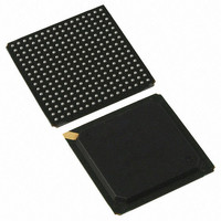
Page 163
... Figure 17-20 Bottom View Drawing The package of PI7C9X130 is a 17mm x 17mm PBGA (256 Pin) package. and the ball size is 0.5mm. PERICOM SEMICONDUCTOR - Confidential The following are the package information and mechanical dimension: Page 163 of 165 PI7C9X130 PCI EXPRESS TO PCI-X BRIDGE The ball pitch is 1.0mm ...
Page 164
... Figure 17-21 Package Outline Drawing 18 ORDERING INFORMATION Device PI7C9X130DNDE PERICOM SEMICONDUCTOR - Confidential Package RoHS Compliant 256-pin PBGA Yes 17 x 17mm Page 164 of 165 PI7C9X130 PCI EXPRESS TO PCI-X BRIDGE Temperature Range -40C to 85C Mar 2010 - Rev 2.0 ...
Page 165
... PCIe Link, REFCLK pin of PI7C9X130 requires a synchronous clock source from the same clock domain of PCIe Root Complex or PCIe End Point that PI7C9X130 is connected to. The requirement of synchronous clock source applies to both Forward and Reverse Mode Operations. PERICOM SEMICONDUCTOR - Confidential PCI EXPRESS TO PCI-X BRIDGE Page 165 of 165 PI7C9X130 Mar 2010 - Rev 2 ...