PI7C9X130DNDE Pericom Semiconductor, PI7C9X130DNDE Datasheet - Page 22
PI7C9X130DNDE
Manufacturer Part Number
PI7C9X130DNDE
Description
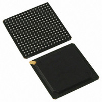
IC PCIE-PCIX BRIDGE 1PORT 256BGA
Manufacturer
Pericom Semiconductor
Specifications of PI7C9X130DNDE
Applications
PCI-to-PCI Bridge
Interface
SMBus (2-Wire/I²C)
Voltage - Supply
1.8V, 3.3V
Package / Case
256-PBGA
Mounting Type
Surface Mount
Operating Temperature (min)
-40C
Operating Temperature Classification
Industrial
Operating Temperature (max)
85C
Package Type
BGA
Rad Hardened
No
Lead Free Status / RoHS Status
Lead free / RoHS Compliant
Available stocks
Company
Part Number
Manufacturer
Quantity
Price
Company:

Part Number:
PI7C9X130DNDE
Manufacturer:
Pericom
Quantity:
135
Company:
Part Number:
PI7C9X130DNDE
Manufacturer:
NSC
Quantity:
70


2.7 POWER AND GROUND PINS
2.8 PIN ASSIGNMENT
PERICOM SEMICONDUCTOR - Confidential
A10
A11
A12
Pin
Figure 2-2 Pin Assignments
A1
A2
A3
A4
A5
A6
A7
A8
A9
VDDA
VDDP
VDDAUX
VTT
VDDA_PLL
VDDP_PLL
VDDC
VDDCAUX
VD33
VAUX
VSS
Name
VDDC
TM0
TM1
PCIXCAP
SMBDAT / SDA
AD[30]
AD[26]
AD[23]
AD[19]
CBE[2]
DEVSEL_L
AD[33]
NAME
ASSIGNMENT
E2, J1, J2, H3
G2, F3, J5, M3,
N2
F4, L1
G1, L5
D3
C2
M5, M6, M11,
M12, J11, H11,
E11, E10, K5,
A1
H5
T1, N4, M7,
M8, M9, L10,
L11, M10, T16,
N13, L12, K12,
K11, J12, H12,
G11, G12, F12,
A16, D13, E12,
F11, E9, E8, E7,
E6, E5
B2
B1, C1, C3, D4,
F5, E1, G5, K3,
K4, L2, N1, M4,
L6, K6, L7, K7,
L8, L9, K8, K9,
K10, J6, J7, J8,
J9, J10, H8, H9,
H10, G10, F10,
F9, F8, F7, F6,
G9, G8, G7, G6,
H7, H6
PIN
E10
E11
E12
Pin
E1
E2
E3
E4
E5
E6
E7
E8
E9
Name
VSS
VDDA
TAN
TAP
VD33
VD33
VD33
VD33
VD33
VDDC
VDDC
VD33
Page 22 of 165
TYPE
P
P
P
P
P
P
P
P
P
P
P
Analog Voltage Supply for PCI Express Interface: Connect to the
1.8V Power Supply.
Digital Voltage Supply for PCI Express Interface: Connect to the
1.8V Power Supply.
Auxiliary Voltage Supply for PCI Express Interface: Connect to the
1.8V Power Supply.
Termination Supply Voltage for PCI Express Interface: Connect to
the 1.8V Power Supply.
Analog Voltage Supply for PLL at PCI Interface: Connect to the
1.8V Power Supply.
Digital Voltage Supply for PLL at PCI Interface: Connect to the
1.8V Power Supply.
Core Supply Voltage: Connect to the 1.8V Power Supply.
Auxiliary Core Supply Voltage: Connect to the 1.8V Power Supply.
I/O Supply Voltage for PCI Interface: Connect to the 3.3V Power
Supply for PCI I/O Buffers.
Auxiliary I/O Supply Voltage for PCI interface: Connect to the 3.3V
Power Supply.
Ground: Connect to Ground.
Pin
J10
J11
J12
J7
J1
J2
J3
J4
J5
J6
J8
J9
Name
VDDA
VDDA
TCN
TCP
VDDP
VSS
VSS
VSS
VSS
VSS
VDDC
VD33
DESCRIPTION
PCI EXPRESS TO PCI-X BRIDGE
Mar 2010 - Rev 2.0
N10
N11
N12
Pin
N1
N2
N3
N4
N5
N6
N7
N8
N9
Name
VSS
VDDP
REQ_L[4] / GPI[2]
VD33
GNT_L[2] / GPO[0]
LOO
RESET_L
GPIO[1]
CLKOUT[2]
CLKOUT[6]
AD[63]
AD[59]
PI7C9X130
Related parts for PI7C9X130DNDE
Image
Part Number
Description
Manufacturer
Datasheet
Request
R

Part Number:
Description:
Fast CMOS bus interface register
Manufacturer:
Pericom Semiconductor
Datasheet:
Part Number:
Description:
4-bit,4-port bus exchange switch
Manufacturer:
Pericom Semiconductor
Datasheet:
Part Number:
Description:
Manufacturer:
Pericom Semiconductor
Datasheet:
Part Number:
Description:
Manufacturer:
Pericom Semiconductor
Datasheet:
Part Number:
Description:
Manufacturer:
Pericom Semiconductor
Datasheet:
Part Number:
Description:
Manufacturer:
Pericom Semiconductor
Datasheet:
Part Number:
Description:
Manufacturer:
Pericom Semiconductor
Datasheet:
Part Number:
Description:
Manufacturer:
Pericom Semiconductor
Datasheet:
Part Number:
Description:
Manufacturer:
Pericom Semiconductor
Datasheet:
Part Number:
Description:
Manufacturer:
Pericom Semiconductor
Datasheet:
Part Number:
Description:
Manufacturer:
Pericom Semiconductor
Datasheet:
Part Number:
Description:
Manufacturer:
Pericom Semiconductor
Datasheet:
Part Number:
Description:
Manufacturer:
Pericom Semiconductor
Datasheet:
Part Number:
Description:
Manufacturer:
Pericom Semiconductor
Datasheet: