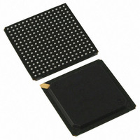
PI7C9X130DNDE Pericom Semiconductor, PI7C9X130DNDE Datasheet - Page 29

PI7C9X130DNDE
Manufacturer Part Number
PI7C9X130DNDE
Description
IC PCIE-PCIX BRIDGE 1PORT 256BGA
Manufacturer
Pericom Semiconductor
Specifications of PI7C9X130DNDE
Applications
PCI-to-PCI Bridge
Interface
SMBus (2-Wire/I²C)
Voltage - Supply
1.8V, 3.3V
Package / Case
256-PBGA
Mounting Type
Surface Mount
Operating Temperature (min)
-40C
Operating Temperature Classification
Industrial
Operating Temperature (max)
85C
Package Type
BGA
Rad Hardened
No
Lead Free Status / RoHS Status
Lead free / RoHS Compliant
Available stocks
Company
Part Number
Manufacturer
Quantity
Price
Company:
Part Number:
PI7C9X130DNDE
Manufacturer:
Pericom
Quantity:
135
Company:
Part Number:
PI7C9X130DNDE
Manufacturer:
NSC
Quantity:
70
6 PCI EXPRESS FUNCTIONAL OVERVIEW
6.1 TLP STRUCTURE
PERICOM SEMICONDUCTOR - Confidential
Figure 5-8 Non-Transparent Registers
PCI Express TLP (Transaction Layer Packet) Structure is comprised of format, type, traffic class,
attributes, TLP digest, TLP poison, and length of data payload.
There are four TLP formats defined in PI7C9X130 based on the states of FMT [1] and FMT [0] as shown
on Table 6-1.
Figure 6-9 TLP Format
Data payload of PI7C9X130 can range from 4 (1DW) to 256 (64DW) bytes. PI7C9X130 supports three
TLP routing mechanisms. They are comprised of Address, ID, and Implicit routings. Address routing
is being used for Memory and IO requests. ID based (bus, device, function numbers) routing is being
Non-transparent Registers
Primary CSR and Memory 0 BAR
Downstream Memory 0 Translated Base
Downstream Memory 0 Setup
Primary CSR I/O BAR
Downstream I/O or Memory 1 BAR
Downstream I/O or Memroy 1 Translated Base
Donwstream I/O or Memroy 1 Setup
Downstream Memory 2 BAR
Downstream Memory 2 Translated Base
Downstream Memory 2 Setup
Downstream Memory 3 BAR
Downstream Memory 2 Setup
Downstream Memory 3 BAR
Downstream Memory 2 Setup
Downstream Memory 3 BAR
Secondary CSR Memory 0 BAR
Upstream Memory 0 Translated Base
Upstream Memory 0 Setup
Secondary CSR I/O BAR
Upstream I/O or Memory 1 BAR
Upstream I/O or Memory 1 Translated Base
Upstream I/O or Memory 1 Setup
Upstream Memory 2 BAR
Upstream Memory 2 Lookup Table Offset
Upstream Memory 2 Lookup Table Data
Upstream Memory 2 Lookup Table (64 32-bit entries)
Upstream Memory 3 BAR
Upstream Memory 3 Upper 32-bit BAR
Upstream Memory 3 Setup
Upstream Memory 3 Upper 32-bit Setup
FMT [1]
0
0
1
1
FMT [0]
0
1
0
1
Page 29 of 165
Typical Access
Configuration access offset 10h
Configuration access offset 98h
Configuration access offset 9Ch
Configuration access offset 14h
Configuration access offset 18h
Configuration access offset A8h
Configuration access offset ACh
Configuration access offset 1Fh
Lower 4K I/O or Memory access offset 008h
Lower 4K I/O or Memory access offset 00Ch
Configuration access offset 23h
Lower 4K I/O or Memory access offset 00Ch
Configuration access offset 23h
Lower 4K I/O or Memory access offset 00Ch
Configuration access offset 23h
Configuration access offset 50h
Configuration access offset E0h
Configuration access offset E4h
Configuration access offset 54h
Configuration access offset ECh
Configuration access offset 5Fh
Lower 4K I/O or Memory access offset 054h
Configuration access offset 63h
Configuration access offset 67h
Lower 4K I/O or Memory access offset 34h
Configuration access offset 58h
Configuration access offset E8h
Lower 4K I/O or Memory access offset 050h
Lower 4K I/O or Memory access offset 100h to 1FFh
Lower 4K I/O or Memory access offset 38h
TLP FORMAT
3 double word, without data
4 double word, without data
3 double word, with data
4 double word, with data
PCI EXPRESS TO PCI-X BRIDGE
Mar 2010 - Rev 2.0
PI7C9X130


