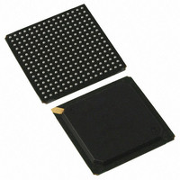
PI7C9X130DNDE Pericom Semiconductor, PI7C9X130DNDE Datasheet - Page 18

PI7C9X130DNDE
Manufacturer Part Number
PI7C9X130DNDE
Description
IC PCIE-PCIX BRIDGE 1PORT 256BGA
Manufacturer
Pericom Semiconductor
Specifications of PI7C9X130DNDE
Applications
PCI-to-PCI Bridge
Interface
SMBus (2-Wire/I²C)
Voltage - Supply
1.8V, 3.3V
Package / Case
256-PBGA
Mounting Type
Surface Mount
Operating Temperature (min)
-40C
Operating Temperature Classification
Industrial
Operating Temperature (max)
85C
Package Type
BGA
Rad Hardened
No
Lead Free Status / RoHS Status
Lead free / RoHS Compliant
Available stocks
Company
Part Number
Manufacturer
Quantity
Price
Company:
Part Number:
PI7C9X130DNDE
Manufacturer:
Pericom
Quantity:
135
Company:
Part Number:
PI7C9X130DNDE
Manufacturer:
NSC
Quantity:
70
2.3 PCI SIGNALS
PERICOM SEMICONDUCTOR - Confidential
AD [31:0]
AD [63:32]
CBE [3:0]
CBE [7:4]
PAR
PAR64
NAME
ASSIGNMENT
D5, A6, B6, C6,
D6, A7, B7, C7,
A8, B8, C8, D8,
A9, B9, C9, D9,
G16, G15, G14,
G13, H16, H15,
H14, H13, J15,
J14, J13, K16,
K15, K14, K13,
L16
N11, P11, R11,
T11, N12, P12,
R12, T12, R13,
T13, P14, R14,
T14, T15, R15,
R16, D16, C15,
C16, B16, B15,
A15, C14, B14,
C13, B13, A13,
D12, C12, B12,
A12, D11
D7, A10, F13,
J16
P13, P15, A14,
C11
F14
D15
PIN
Page 18 of 165
TYPE
B
B
B
B
B
B
Address / Data: Multiplexed address and data bus. Address phase is
aligned with first clock of FRAME_L assertion. Data phase is aligned
with IRDY_L or TRDY_L assertion. Data is transferred on rising edges
of FBCLKIN when both IRDY_L and TRDY_L are asserted. During bus
idle (both FRAME_L and IRDY_L are de-asserted), PI7C9X130 drives
AD [31:0] to a valid logic level when arbiter is parking to PI7C9X130
on PCI bus.
Upper 32-bit Address / Data: Multiplexed address and data bus.
Address phase is aligned with first clock of FRAME_L assertion. Data
phase is aligned with IRDY_L or TRDY_L assertion. Data is transferred
on rising edges of FBCLKIN when both IRDY_L and TRDY_L are
asserted. During bus idle (both FRAME_L and IRDY_L are de-
asserted), PI7C9X130 drives AD [63:32] to a valid logic level when
arbiter is parking to PI7C9X130 on PCI bus.
Command / Byte Enables (Active LOW): Multiplexed command at
address phase and byte enable at data phase. During address phase, the
initiator drives commands on CBE [3:0] signals to start the transaction.
If the command is a write transaction, the initiator will drive the byte
enables during data phase. Otherwise, the target will drive the byte
enables during data phase. During bus idle, PI7C9X130 drives CBE
[3:0] signals to a valid logic level when arbiter is parking to PI7C9X130
on PCI bus.
Upper 4-bit Command / Byte Enables (Active LOW): Multiplexed
command at address phase and byte enable at data phase. During address
phase, the initiator drives commands on CBE [3:0] signals to start the
transaction. If the command is a write transaction, the initiator will drive
the byte enables during data phase. Otherwise, the target will drive the
byte enables during data phase. During bus idle, PI7C9X130 drives
CBE [7:4] signals to a valid logic level when arbiter is parking to
PI7C9X130 on PCI bus.
Parity Bit: Parity bit is an even parity (i.e. even number of 1’s),
which generates based on the values of AD [31:0], CBE [3:0]. If
PI7C9X130 is an initiator with a write transaction, PI7C9X130 will tri-
state PAR. If PI7C9X130 is a target and a write transaction,
PI7C9X130 will drive PAR one clock after the address or data phase.
If PI7C9X130 is a target and a read transaction, PI7C9X130 will drive
PAR one clock after the address phase and tri-state PAR during data
phases. PAR is tri-stated one cycle after the AD lines are tri-stated.
During bus idle, PI7C9X130 drives PAR to a valid logic level when
arbiter is parking to PI7C9X130 on PCI bus.
Parity Bit for Upper 32-bit: Parity bit is an even parity (i.e. even
number of 1’s), which generates based on the values of AD [63:32],
CBE [7:4]. If PI7C9X130 is an initiator with a write transaction,
PI7C9X130 will tri-state PAR64. If PI7C9X130 is a target and a write
transaction, PI7C9X130 will drive PAR64 one clock after the address or
data phase. If PI7C9X130 is a target and a read transaction,
PI7C9X130 will drive PAR64 one clock after the address phase and tri-
state PAR64 during data phases. PAR64 is tri-stated one cycle after the
AD lines are tri-stated. During bus idle, PI7C9X130 drives PAR64 to a
valid logic level when arbiter is parking to PI7C9X130 on PCI bus.
DESCRIPTION
PCI EXPRESS TO PCI-X BRIDGE
Mar 2010 - Rev 2.0
PI7C9X130


