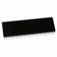
Z8018010PSG Zilog, Z8018010PSG Datasheet - Page 164

Z8018010PSG
Manufacturer Part Number
Z8018010PSG
Description
IC 10MHZ Z180 CMOS ENH MPU 64DIP
Manufacturer
Zilog
Specifications of Z8018010PSG
Processor Type
Z180
Features
8-Bit, Enhanced Z80 Megacell
Speed
10MHz
Voltage
5V
Mounting Type
Through Hole
Package / Case
64-DIP (0.750", 19.05mm)
Processor Series
Z8018xx
Core
Z80
Data Bus Width
8 bit
Maximum Clock Frequency
10 MHz
Number Of Timers
2
Operating Supply Voltage
0 V to 5 V
Maximum Operating Temperature
+ 70 C
Mounting Style
Through Hole
Minimum Operating Temperature
0 C
Core Size
8bit
Cpu Speed
10MHz
Digital Ic Case Style
DIP
No. Of Pins
64
Supply Voltage Range
4.5V To 5.5V
Operating Temperature Range
0°C To +70°C
Svhc
No SVHC (18-Jun-2010)
Base Number
8018010
Rohs Compliant
Yes
Clock Frequency
10MHz
Lead Free Status / RoHS Status
Lead free / RoHS Compliant
Other names
269-3889
Z8018010PSG
Z8018010PSG
Available stocks
Company
Part Number
Manufacturer
Quantity
Price
Company:
Part Number:
Z8018010PSG
Manufacturer:
Zilog
Quantity:
40
- Current page: 164 of 326
- Download datasheet (5Mb)
Bit
Position Bit/Field R/W
4
2
–
0
TE
SS2
–
0
CSI/O Transmit/Receive Data Register (TRDR: I/O
Address = 0BH).
TRDR is used for both CSI/O transmission and reception. Thus, the
system design must insure that the constraints of half-duplex operation
are met (Transmit and receive operation cannot occur simultaneously).
For example, if a CSI/O transmission is attempted while the CSI/O is
receiving data, the CSI/O does not work.
TRDR is not buffered. Attempting to perform a CSI/O transmit while the
previous transmit data is still being shifted out causes the shift data to be
immediately updated, thereby corrupting the transmit operation in
progress. Similarly, reading TRDR during a transmit or receive must be
avoided.
R/W
R/W
Value
Description
Transmit Enable — A CSI/O transmit operation is
started by setting TE to 1. When TE is set to 1, the data
clock is enabled. When in internal clock mode, the data
clock is output from the CKS pin. In external clock mode,
the clock is input on the CKS pin. In either case, data is
shifted out on the TXS pin synchronous with the (internal
or external) data clock. After transmitting 8 bits of data,
the CSI/O automatically clears TE to 0, EF is set to 1, and
an interrupt (if enabled by EIE = 1) is generated. TE and
RE are never both set to 1 at the same time. TE is cleared
to 0 during RESET and IOSTOP mode.
Speed Select — Selects the CSI/O transmit/receive clock
source and speed. SS2, SS I and SS0 are all set to 1 during
RESET. Table 22 shows CSI/O Baud Rate Selection.
Family MPU User Manual
UM005003-0703
Z8018x
149
Related parts for Z8018010PSG
Image
Part Number
Description
Manufacturer
Datasheet
Request
R

Part Number:
Description:
Microprocessor Unit
Manufacturer:
ZiLOG Semiconductor
Datasheet:

Part Number:
Description:
Z80180 EMULATOR
Manufacturer:
Zilog
Datasheet:

Part Number:
Description:
Z80180, Z8s180, Z8l180 Mpu Operation
Manufacturer:
ZiLOG Semiconductor
Datasheet:

Part Number:
Description:
Communication Controllers, ZILOG INTELLIGENT PERIPHERAL CONTROLLER (ZIP)
Manufacturer:
Zilog, Inc.
Datasheet:

Part Number:
Description:
KIT DEV FOR Z8 ENCORE 16K TO 64K
Manufacturer:
Zilog
Datasheet:

Part Number:
Description:
KIT DEV Z8 ENCORE XP 28-PIN
Manufacturer:
Zilog
Datasheet:

Part Number:
Description:
DEV KIT FOR Z8 ENCORE 8K/4K
Manufacturer:
Zilog
Datasheet:

Part Number:
Description:
KIT DEV Z8 ENCORE XP 28-PIN
Manufacturer:
Zilog
Datasheet:

Part Number:
Description:
DEV KIT FOR Z8 ENCORE 4K TO 8K
Manufacturer:
Zilog
Datasheet:

Part Number:
Description:
CMOS Z8 microcontroller. ROM 16 Kbytes, RAM 256 bytes, speed 16 MHz, 32 lines I/O, 3.0V to 5.5V
Manufacturer:
Zilog, Inc.
Datasheet:

Part Number:
Description:
Low-cost microcontroller. 512 bytes ROM, 61 bytes RAM, 8 MHz
Manufacturer:
Zilog, Inc.
Datasheet:

Part Number:
Description:
Z8 4K OTP Microcontroller
Manufacturer:
Zilog, Inc.
Datasheet:

Part Number:
Description:
CMOS SUPER8 ROMLESS MCU
Manufacturer:
Zilog, Inc.
Datasheet:

Part Number:
Description:
SL1866 CMOSZ8 OTP Microcontroller
Manufacturer:
Zilog, Inc.
Datasheet:


