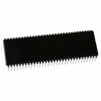
Z8018010PSG Zilog, Z8018010PSG Datasheet - Page 124

Z8018010PSG
Manufacturer Part Number
Z8018010PSG
Description
IC 10MHZ Z180 CMOS ENH MPU 64DIP
Manufacturer
Zilog
Specifications of Z8018010PSG
Processor Type
Z180
Features
8-Bit, Enhanced Z80 Megacell
Speed
10MHz
Voltage
5V
Mounting Type
Through Hole
Package / Case
64-DIP (0.750", 19.05mm)
Processor Series
Z8018xx
Core
Z80
Data Bus Width
8 bit
Maximum Clock Frequency
10 MHz
Number Of Timers
2
Operating Supply Voltage
0 V to 5 V
Maximum Operating Temperature
+ 70 C
Mounting Style
Through Hole
Minimum Operating Temperature
0 C
Core Size
8bit
Cpu Speed
10MHz
Digital Ic Case Style
DIP
No. Of Pins
64
Supply Voltage Range
4.5V To 5.5V
Operating Temperature Range
0°C To +70°C
Svhc
No SVHC (18-Jun-2010)
Base Number
8018010
Rohs Compliant
Yes
Clock Frequency
10MHz
Lead Free Status / RoHS Status
Lead free / RoHS Compliant
Other names
269-3889
Z8018010PSG
Z8018010PSG
Available stocks
Company
Part Number
Manufacturer
Quantity
Price
Company:
Part Number:
Z8018010PSG
Manufacturer:
Zilog
Quantity:
40
- Current page: 124 of 326
- Download datasheet (5Mb)
memory mapped I/O. transfers, the CKA0/DREQ0 pin automatically
functions as input pin or output pin even if it has been programmed as
output pin for CKA0. And the CKA1/TEND0 pin functions as an input or
an output pin for TEND0 by setting CKA1D to 1 in CNTLA1.
To initiate memory to/from I/O (and memory to/from memory mapped
I/O) DMA transfer for channel 0, perform the following operations:
1. Load the memory and I/O or memory mapped I/O source and
2. Specify memory to/from I/O or memory to/from memory mapped I/O
3. Load the number of bytes to transfer in BCR0.
4. Specify whether DREQ0 is edge- or level-sense by programming the
5. Enable or disable DMA termination interrupt with the DIE0 bit in
6. Program DE0: = 1 (with DWEO = 0 in the same access) in DSTAT
Memory to ASCI - Channel 0
Channel 0 has extra capability to support DMA transfer to/from the on-
chip two channel ASCI. In this case, the external DREQ0 input is not
used for DMA timing. Rather, the ASCI status bits are used to generate an
internal DREQ0 The TDRE (Transmit Data Register Empty) bit and the
RDRF (Receive Data Register Full) bit are used to generate an internal
destination addresses into SAR0 and DAR0.
I/O addresses (not memory mapped I/O are limited to 16 bits (A0–
A15). Make sure that bits A16, A17 and A19 are
care) to correctly enable the external DREQ0 input.
mode and address increment/decrement in the SM0, SM1, DM0 and
DM1 bits of DMODE.
DMS0 bit of DCNTL.
DSTAT.
and the DMA operation begins under the control of the DREQ0 input.
Family MPU User Manual
0
(A18 is a don't
UM005003-0703
Z8018x
109
Related parts for Z8018010PSG
Image
Part Number
Description
Manufacturer
Datasheet
Request
R

Part Number:
Description:
Microprocessor Unit
Manufacturer:
ZiLOG Semiconductor
Datasheet:

Part Number:
Description:
Z80180 EMULATOR
Manufacturer:
Zilog
Datasheet:

Part Number:
Description:
Z80180, Z8s180, Z8l180 Mpu Operation
Manufacturer:
ZiLOG Semiconductor
Datasheet:

Part Number:
Description:
Communication Controllers, ZILOG INTELLIGENT PERIPHERAL CONTROLLER (ZIP)
Manufacturer:
Zilog, Inc.
Datasheet:

Part Number:
Description:
KIT DEV FOR Z8 ENCORE 16K TO 64K
Manufacturer:
Zilog
Datasheet:

Part Number:
Description:
KIT DEV Z8 ENCORE XP 28-PIN
Manufacturer:
Zilog
Datasheet:

Part Number:
Description:
DEV KIT FOR Z8 ENCORE 8K/4K
Manufacturer:
Zilog
Datasheet:

Part Number:
Description:
KIT DEV Z8 ENCORE XP 28-PIN
Manufacturer:
Zilog
Datasheet:

Part Number:
Description:
DEV KIT FOR Z8 ENCORE 4K TO 8K
Manufacturer:
Zilog
Datasheet:

Part Number:
Description:
CMOS Z8 microcontroller. ROM 16 Kbytes, RAM 256 bytes, speed 16 MHz, 32 lines I/O, 3.0V to 5.5V
Manufacturer:
Zilog, Inc.
Datasheet:

Part Number:
Description:
Low-cost microcontroller. 512 bytes ROM, 61 bytes RAM, 8 MHz
Manufacturer:
Zilog, Inc.
Datasheet:

Part Number:
Description:
Z8 4K OTP Microcontroller
Manufacturer:
Zilog, Inc.
Datasheet:

Part Number:
Description:
CMOS SUPER8 ROMLESS MCU
Manufacturer:
Zilog, Inc.
Datasheet:

Part Number:
Description:
SL1866 CMOSZ8 OTP Microcontroller
Manufacturer:
Zilog, Inc.
Datasheet:


