Z8018010PSG Zilog, Z8018010PSG Datasheet - Page 163
Z8018010PSG
Manufacturer Part Number
Z8018010PSG
Description
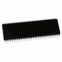
IC 10MHZ Z180 CMOS ENH MPU 64DIP
Manufacturer
Zilog
Specifications of Z8018010PSG
Processor Type
Z180
Features
8-Bit, Enhanced Z80 Megacell
Speed
10MHz
Voltage
5V
Mounting Type
Through Hole
Package / Case
64-DIP (0.750", 19.05mm)
Processor Series
Z8018xx
Core
Z80
Data Bus Width
8 bit
Maximum Clock Frequency
10 MHz
Number Of Timers
2
Operating Supply Voltage
0 V to 5 V
Maximum Operating Temperature
+ 70 C
Mounting Style
Through Hole
Minimum Operating Temperature
0 C
Core Size
8bit
Cpu Speed
10MHz
Digital Ic Case Style
DIP
No. Of Pins
64
Supply Voltage Range
4.5V To 5.5V
Operating Temperature Range
0°C To +70°C
Svhc
No SVHC (18-Jun-2010)
Base Number
8018010
Rohs Compliant
Yes
Clock Frequency
10MHz
Lead Free Status / RoHS Status
Lead free / RoHS Compliant
Other names
269-3889
Z8018010PSG
Z8018010PSG
Available stocks
Company
Part Number
Manufacturer
Quantity
Price
Company:

Part Number:
Z8018010PSG
Manufacturer:
Zilog
Quantity:
40


148
UM005003-0703
Bit
Position Bit/Field R/W
7
6
5
Z8018x
Family MPU User Manual
EF
EIE
RE
R
R/W
R/W
Value
Description
End Flag — EF is set to 1 by the CSI/O to indicate
completion of an 8-bit data transmit or receive operation.
If EIE (End Interrupt Enable) bit = 1 when EF is set to 1, a
CPU interrupt request is generated. Program access of
TRDR only occurs if EF is 1. The CSI/O clears EF to 0
when TRDR is read or written. EF is cleared to 0 during
RESET and IOSTOP mode.
End Interrupt Enable — EIE is set to 1 to enable EF = 1
to generate a CPU interrupt request. The interrupt request
is inhibited if EIE is reset to 0. EIE is cleared to 0 during
RESET.
Receive Enable — A CSI/O receive operation is started
by setting RE to 1. When RE is set to 1, the data clock is
enabled. In internal clock mode, the data clock is output
from the CKS pin. In external dock mode, the dock is
input on the CKS pin. In either case, data is shifted in on
the RXS pin in synchronization with the (internal or
external) data clock. After receiving 8 bits of data, the
CSI/O automatically clears RE to 0, EF is set to 1, and an
interrupt (if enabled by EIE = 1) is generated. RE and TE
are never both set to 1 at the same time. RE is cleared to 0
during RESET and ISTOP mode.
RXS is multiplexed with CTS1 modem control input of
ASCI channel 1. In order to enable the RXS function, the
CTS1E bit in CNTA1 must be reset to 0.
Related parts for Z8018010PSG
Image
Part Number
Description
Manufacturer
Datasheet
Request
R

Part Number:
Description:
Microprocessor Unit
Manufacturer:
ZiLOG Semiconductor
Datasheet:

Part Number:
Description:
Z80180 EMULATOR
Manufacturer:
Zilog
Datasheet:
Part Number:
Description:
Z80180, Z8s180, Z8l180 Mpu Operation
Manufacturer:
ZiLOG Semiconductor
Datasheet:

Part Number:
Description:
Communication Controllers, ZILOG INTELLIGENT PERIPHERAL CONTROLLER (ZIP)
Manufacturer:
Zilog, Inc.
Datasheet:

Part Number:
Description:
KIT DEV FOR Z8 ENCORE 16K TO 64K
Manufacturer:
Zilog
Datasheet:

Part Number:
Description:
KIT DEV Z8 ENCORE XP 28-PIN
Manufacturer:
Zilog
Datasheet:

Part Number:
Description:
DEV KIT FOR Z8 ENCORE 8K/4K
Manufacturer:
Zilog
Datasheet:

Part Number:
Description:
KIT DEV Z8 ENCORE XP 28-PIN
Manufacturer:
Zilog
Datasheet:
Part Number:
Description:
DEV KIT FOR Z8 ENCORE 4K TO 8K
Manufacturer:
Zilog
Datasheet:
Part Number:
Description:
CMOS Z8 microcontroller. ROM 16 Kbytes, RAM 256 bytes, speed 16 MHz, 32 lines I/O, 3.0V to 5.5V
Manufacturer:
Zilog, Inc.
Datasheet:
Part Number:
Description:
Low-cost microcontroller. 512 bytes ROM, 61 bytes RAM, 8 MHz
Manufacturer:
Zilog, Inc.
Datasheet:
Part Number:
Description:
Z8 4K OTP Microcontroller
Manufacturer:
Zilog, Inc.
Datasheet:
Part Number:
Description:
CMOS SUPER8 ROMLESS MCU
Manufacturer:
Zilog, Inc.
Datasheet:
Part Number:
Description:
SL1866 CMOSZ8 OTP Microcontroller
Manufacturer:
Zilog, Inc.
Datasheet: