ATMEGA64A-MNR Atmel, ATMEGA64A-MNR Datasheet - Page 87
ATMEGA64A-MNR
Manufacturer Part Number
ATMEGA64A-MNR
Description
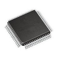
IC MCU AVR 64K FLASH 8QFN
Manufacturer
Atmel
Series
AVR® ATmegar
Datasheet
1.ATMEGA64A-AU.pdf
(392 pages)
Specifications of ATMEGA64A-MNR
Core Processor
AVR
Core Size
8-Bit
Speed
16MHz
Connectivity
I²C, SPI, UART/USART
Peripherals
Brown-out Detect/Reset, POR, PWM, WDT
Number Of I /o
53
Program Memory Size
64KB (32K x 16)
Program Memory Type
FLASH
Eeprom Size
2K x 8
Ram Size
4K x 8
Voltage - Supply (vcc/vdd)
2.7 V ~ 5.5 V
Data Converters
A/D 8x10b
Oscillator Type
Internal
Operating Temperature
-40°C ~ 85°C
Package / Case
*
Core
AVR8
Data Bus Width
8 bit
Data Ram Size
2 KB
Interface Type
SPI, UART, I2C
Maximum Clock Frequency
16 MHz
Number Of Programmable I/os
53
Operating Supply Voltage
2.7 V to 5.5 V
Maximum Operating Temperature
+ 105 C
Mounting Style
SMD/SMT
Operating Temperature Range
- 40 C to + 85 C
Processor To Be Evaluated
ATMEGA64A
Lead Free Status / RoHS Status
Lead free / RoHS Compliant


13.3.7
8160C–AVR–07/09
Alternate Functions of Port G
Table 13-20. Overriding Signals for Alternate Functions in PF3:PF0
In ATmega103 compatibility mode, only the alternate functions are the defaults for Port G, and
Port G cannot be used as General Digital Port Pins. The alternate pin configuration is as follows:
Table 13-21. Port G Pins Alternate Functions
• TOSC1 – Port G, Bit 4
TOSC2, Timer Oscillator pin 1: When the AS0 bit in ASSR is set (one) to enable asynchronous
clocking of Timer/Counter0, pin PG4 is disconnected from the port, and becomes the inverting
output of the Oscillator amplifier. In this mode, a crystal Oscillator is connected to this pin, and
the pin can not be used as an I/O pin.
• TOSC2 – Port G, Bit 3
TOSC2, Timer Oscillator pin 2: When the AS0 bit in ASSR is set (one) to enable asynchronous
clocking of Timer/Counter0, pin PG3 is disconnected from the port, and becomes the input of the
inverting Oscillator amplifier. In this mode, a crystal Oscillator is connected to this pin, and the
pin cannot be used as an I/O pin.
• ALE – Port G, Bit 2
ALE is the external data memory Address Latch Enable signal.
• RD – Port G, Bit 1
RD is the external data memory read control strobe.
Signal
Name
PUOE
PUOV
DDOE
DDOV
PVOE
PVOV
DIEOE
DIEOV
DI
AIO
Port Pin
PG4
PG3
PG2
PG1
PG0
PF3/ADC3
0
0
0
0
0
0
0
0
–
ADC3 INPUT
Alternate Function
TOSC1 (RTC Oscillator Timer/Counter0)
TOSC2 (RTC Oscillator Timer/Counter0)
ALE (Address Latch Enable to external memory)
RD (Read strobe to external memory)
WR (Write strobe to external memory)
PF2/ADC2
0
0
0
0
0
0
0
0
–
ADC2 INPUT
PF1/ADC1
0
0
0
0
0
0
0
0
–
ADC1 INPUT
ATmega64A
PF0/ADC0
0
0
0
0
0
0
0
0
–
ADC0 INPUT
87
Related parts for ATMEGA64A-MNR
Image
Part Number
Description
Manufacturer
Datasheet
Request
R

Part Number:
Description:
Manufacturer:
Atmel Corporation
Datasheet:
Part Number:
Description:
Manufacturer:
ATMEL Corporation
Datasheet:
Part Number:
Description:
Manufacturer:
ATMEL Corporation
Datasheet:

Part Number:
Description:
IC AVR MCU 64K 16MHZ 5V 64TQFP
Manufacturer:
Atmel
Datasheet:

Part Number:
Description:
IC AVR MCU 64K 16MHZ 5V 64-QFN
Manufacturer:
Atmel
Datasheet:
Part Number:
Description:
IC AVR MCU 64K 16MHZ COM 64-TQFP
Manufacturer:
Atmel
Datasheet:
Part Number:
Description:
IC AVR MCU 64K 16MHZ IND 64-TQFP
Manufacturer:
Atmel
Datasheet:

Part Number:
Description:
IC AVR MCU 64K 16MHZ COM 64-QFN
Manufacturer:
Atmel
Datasheet:
Part Number:
Description:
MCU AVR 64KB FLASH 16MHZ 64TQFP
Manufacturer:
Atmel
Datasheet:
Part Number:
Description:
MCU AVR 64KB FLASH 16MHZ 64QFN
Manufacturer:
Atmel
Datasheet:
Part Number:
Description:
IC AVR MCU 64K 16MHZ IND 64-QFN
Manufacturer:
Atmel
Datasheet:
Part Number:
Description:
IC MCU AVR 64K 5V 16MHZ 64-TQFP
Manufacturer:
Atmel
Datasheet:
Part Number:
Description:
IC MCU AVR 64K 5V 16MHZ 64-QFN
Manufacturer:
Atmel
Datasheet:
Part Number:
Description:
MCU 8-Bit ATmega AVR RISC 64KB Flash 5V 64-Pin TQFP T/R
Manufacturer:
Atmel
Datasheet: