ATMEGA64A-MNR Atmel, ATMEGA64A-MNR Datasheet - Page 81
ATMEGA64A-MNR
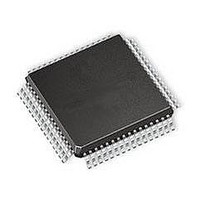
Manufacturer Part Number
ATMEGA64A-MNR
Description
IC MCU AVR 64K FLASH 8QFN
Manufacturer
Atmel
Series
AVR® ATmegar
Datasheet
1.ATMEGA64A-AU.pdf
(392 pages)
Specifications of ATMEGA64A-MNR
Core Processor
AVR
Core Size
8-Bit
Speed
16MHz
Connectivity
I²C, SPI, UART/USART
Peripherals
Brown-out Detect/Reset, POR, PWM, WDT
Number Of I /o
53
Program Memory Size
64KB (32K x 16)
Program Memory Type
FLASH
Eeprom Size
2K x 8
Ram Size
4K x 8
Voltage - Supply (vcc/vdd)
2.7 V ~ 5.5 V
Data Converters
A/D 8x10b
Oscillator Type
Internal
Operating Temperature
-40°C ~ 85°C
Package / Case
*
Core
AVR8
Data Bus Width
8 bit
Data Ram Size
2 KB
Interface Type
SPI, UART, I2C
Maximum Clock Frequency
16 MHz
Number Of Programmable I/os
53
Operating Supply Voltage
2.7 V to 5.5 V
Maximum Operating Temperature
+ 105 C
Mounting Style
SMD/SMT
Operating Temperature Range
- 40 C to + 85 C
Processor To Be Evaluated
ATMEGA64A
Lead Free Status / RoHS Status
Lead free / RoHS Compliant


8160C–AVR–07/09
• INT3/TXD1 – Port D, Bit 3
INT3, External Interrupt Source 3: The PD3 pin can serve as an External Interrupt source to the
MCU.
TXD1, Transmit Data (Data output pin for the USART1). When the USART1 transmitter is
enabled, this pin is configured as an output regardless of the value of DDD3.
• INT2/RXD1 – Port D, Bit 2
INT2, External Interrupt source 2. The PD2 pin can serve as an External Interrupt source to the
MCU.
RXD1, Receive Data (Data input pin for the USART1). When the USART1 receiver is enabled
this pin is configured as an input regardless of the value of DDD2. When the USART forces this
pin to be an input, the pull-up can still be controlled by the PORTD2 bit.
• INT1/SDA – Port D, Bit 1
INT1, External Interrupt Source 1. The PD1 pin can serve as an External Interrupt source to the
MCU.
SDA, Two-wire Serial Interface Data: When the TWEN bit in TWCR is set (one) to enable the
Two-wire Serial Interface, pin PD1 is disconnected from the port and becomes the serial data I/O
pin for the Two-wire Serial Interface. In this mode, there is a spike filter on the pin to suppress
spikes shorter than 50 ns on the input signal, and the pin is driven by an open drain driver with
slew-rate limitation.
• INT0/SCL – Port D, Bit 0
INT0, External Interrupt Source 0. The PD0 pin can serve as an External Interrupt source to the
MCU.
SCL, Two-wire Serial Interface Clock: When the TWEN bit in TWCR is set (one) to enable the
Two-wire Serial Interface, pin PD0 is disconnected from the port and becomes the serial clock
I/O pin for the Two-wire Serial Interface. In this mode, there is a spike filter on the pin to sup-
press spikes shorter than 50 ns on the input signal, and the pin is driven by an open drain driver
with slew-rate limitation.
Table 13-13
shown in
Figure 13-5 on page
and
Table 13-14
relates the alternate functions of Port D to the overriding signals
73.
ATmega64A
81
Related parts for ATMEGA64A-MNR
Image
Part Number
Description
Manufacturer
Datasheet
Request
R

Part Number:
Description:
Manufacturer:
Atmel Corporation
Datasheet:
Part Number:
Description:
Manufacturer:
ATMEL Corporation
Datasheet:
Part Number:
Description:
Manufacturer:
ATMEL Corporation
Datasheet:

Part Number:
Description:
IC AVR MCU 64K 16MHZ 5V 64TQFP
Manufacturer:
Atmel
Datasheet:

Part Number:
Description:
IC AVR MCU 64K 16MHZ 5V 64-QFN
Manufacturer:
Atmel
Datasheet:
Part Number:
Description:
IC AVR MCU 64K 16MHZ COM 64-TQFP
Manufacturer:
Atmel
Datasheet:
Part Number:
Description:
IC AVR MCU 64K 16MHZ IND 64-TQFP
Manufacturer:
Atmel
Datasheet:

Part Number:
Description:
IC AVR MCU 64K 16MHZ COM 64-QFN
Manufacturer:
Atmel
Datasheet:
Part Number:
Description:
MCU AVR 64KB FLASH 16MHZ 64TQFP
Manufacturer:
Atmel
Datasheet:
Part Number:
Description:
MCU AVR 64KB FLASH 16MHZ 64QFN
Manufacturer:
Atmel
Datasheet:
Part Number:
Description:
IC AVR MCU 64K 16MHZ IND 64-QFN
Manufacturer:
Atmel
Datasheet:
Part Number:
Description:
IC MCU AVR 64K 5V 16MHZ 64-TQFP
Manufacturer:
Atmel
Datasheet:
Part Number:
Description:
IC MCU AVR 64K 5V 16MHZ 64-QFN
Manufacturer:
Atmel
Datasheet:
Part Number:
Description:
MCU 8-Bit ATmega AVR RISC 64KB Flash 5V 64-Pin TQFP T/R
Manufacturer:
Atmel
Datasheet: