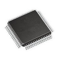
ATMEGA64A-MNR Atmel, ATMEGA64A-MNR Datasheet - Page 76

ATMEGA64A-MNR
Manufacturer Part Number
ATMEGA64A-MNR
Description
IC MCU AVR 64K FLASH 8QFN
Manufacturer
Atmel
Series
AVR® ATmegar
Datasheet
1.ATMEGA64A-AU.pdf
(392 pages)
Specifications of ATMEGA64A-MNR
Core Processor
AVR
Core Size
8-Bit
Speed
16MHz
Connectivity
I²C, SPI, UART/USART
Peripherals
Brown-out Detect/Reset, POR, PWM, WDT
Number Of I /o
53
Program Memory Size
64KB (32K x 16)
Program Memory Type
FLASH
Eeprom Size
2K x 8
Ram Size
4K x 8
Voltage - Supply (vcc/vdd)
2.7 V ~ 5.5 V
Data Converters
A/D 8x10b
Oscillator Type
Internal
Operating Temperature
-40°C ~ 85°C
Package / Case
*
Core
AVR8
Data Bus Width
8 bit
Data Ram Size
2 KB
Interface Type
SPI, UART, I2C
Maximum Clock Frequency
16 MHz
Number Of Programmable I/os
53
Operating Supply Voltage
2.7 V to 5.5 V
Maximum Operating Temperature
+ 105 C
Mounting Style
SMD/SMT
Operating Temperature Range
- 40 C to + 85 C
Processor To Be Evaluated
ATMEGA64A
Lead Free Status / RoHS Status
Lead free / RoHS Compliant
- Current page: 76 of 392
- Download datasheet (8Mb)
13.3.2
8160C–AVR–07/09
Alternate Functions of Port B
Table 13-5.
Note:
The Port B pins with alternate functions are shown in
Table 13-6.
Note:
The alternate pin configuration is as follows:
• OC2/OC1C, Bit 7
OC2, Output Compare Match output: The PB7 pin can serve as an external output for the
Timer/Counter2 Output Compare. The pin has to be configured as an output (DDB7 set (one)) to
serve this function. The OC2 pin is also the output pin for the PWM mode timer function.
OC1C, Output Compare Match C output: The PB7 pin can serve as an external output for the
Timer/Counter1 Output Compare C. The pin has to be configured as an output (DDB7 set (one))
to serve this function. The OC1C pin is also the output pin for the PWM mode timer function.
Signal
Name
PUOE
PUOV
DDOE
DDOV
PVOE
PVOV
DIEOE
DIEOV
DI
AIO
Port Pin
PB7
PB6
PB5
PB4
PB3
PB2
PB1
PB0
1. ADA is short for ADdress Active and represents the time when address is output. See
1. OC1C not applicable in ATmega103 compatibility mode.
nal Memory Interface” on page 23
Alternate Functions
OC2/OC1C
and PWM Output C for Timer/Counter1)
OC1B (Output Compare and PWM Output B for Timer/Counter1)
OC1A (Output Compare and PWM Output A for Timer/Counter1)
OC0 (Output Compare and PWM Output for Timer/Counter0)
MISO (SPI Bus Master Input/Slave Output)
MOSI (SPI Bus Master Output/Slave Input)
SCK (SPI Bus Serial Clock)
SS (SPI Slave Select input)
Overriding Signals for Alternate Functions in PA3:PA0
Port B Pins Alternate Functions
PORTA3 • PUD
OUTPUT • WR
~(WR | ADA) •
A3 • ADA | D3
PA3/AD3
D3 INPUT
WR | ADA
SRE
SRE
SRE
0
0
–
(1)
(Output Compare and PWM Output for Timer/Counter2 or Output Compare
PORTA2 • PUD
OUTPUT • WR
~(WR | ADA) •
A2• ADA | D2
PA2/AD2
D2 INPUT
WR | ADA
SRE
SRE
SRE
0
0
–
for details.
Table
PORTA1 • PUD
OUTPUT • WR
~(WR | ADA) •
A1 • ADA | D1
PA1/AD1
13-6.
WR | ADA
D1 INPUT
SRE
SRE
SRE
0
0
–
(1)
ATmega64A
PORTA0 • PUD
OUTPUT • WR
~(WR | ADA) •
A0 • ADA | D0
PA0/AD0
WR | ADA
D0 INPUT
SRE
SRE
SRE
0
0
–
“Exter-
76
Related parts for ATMEGA64A-MNR
Image
Part Number
Description
Manufacturer
Datasheet
Request
R

Part Number:
Description:
Manufacturer:
Atmel Corporation
Datasheet:

Part Number:
Description:
Manufacturer:
ATMEL Corporation
Datasheet:

Part Number:
Description:
Manufacturer:
ATMEL Corporation
Datasheet:

Part Number:
Description:
IC AVR MCU 64K 16MHZ 5V 64TQFP
Manufacturer:
Atmel
Datasheet:

Part Number:
Description:
IC AVR MCU 64K 16MHZ 5V 64-QFN
Manufacturer:
Atmel
Datasheet:

Part Number:
Description:
IC AVR MCU 64K 16MHZ COM 64-TQFP
Manufacturer:
Atmel
Datasheet:

Part Number:
Description:
IC AVR MCU 64K 16MHZ IND 64-TQFP
Manufacturer:
Atmel
Datasheet:

Part Number:
Description:
IC AVR MCU 64K 16MHZ COM 64-QFN
Manufacturer:
Atmel
Datasheet:

Part Number:
Description:
MCU AVR 64KB FLASH 16MHZ 64TQFP
Manufacturer:
Atmel
Datasheet:

Part Number:
Description:
MCU AVR 64KB FLASH 16MHZ 64QFN
Manufacturer:
Atmel
Datasheet:

Part Number:
Description:
IC AVR MCU 64K 16MHZ IND 64-QFN
Manufacturer:
Atmel
Datasheet:

Part Number:
Description:
IC MCU AVR 64K 5V 16MHZ 64-TQFP
Manufacturer:
Atmel
Datasheet:

Part Number:
Description:
IC MCU AVR 64K 5V 16MHZ 64-QFN
Manufacturer:
Atmel
Datasheet:

Part Number:
Description:
MCU 8-Bit ATmega AVR RISC 64KB Flash 5V 64-Pin TQFP T/R
Manufacturer:
Atmel
Datasheet:


