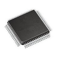
ATMEGA64A-MNR Atmel, ATMEGA64A-MNR Datasheet - Page 27

ATMEGA64A-MNR
Manufacturer Part Number
ATMEGA64A-MNR
Description
IC MCU AVR 64K FLASH 8QFN
Manufacturer
Atmel
Series
AVR® ATmegar
Datasheet
1.ATMEGA64A-AU.pdf
(392 pages)
Specifications of ATMEGA64A-MNR
Core Processor
AVR
Core Size
8-Bit
Speed
16MHz
Connectivity
I²C, SPI, UART/USART
Peripherals
Brown-out Detect/Reset, POR, PWM, WDT
Number Of I /o
53
Program Memory Size
64KB (32K x 16)
Program Memory Type
FLASH
Eeprom Size
2K x 8
Ram Size
4K x 8
Voltage - Supply (vcc/vdd)
2.7 V ~ 5.5 V
Data Converters
A/D 8x10b
Oscillator Type
Internal
Operating Temperature
-40°C ~ 85°C
Package / Case
*
Core
AVR8
Data Bus Width
8 bit
Data Ram Size
2 KB
Interface Type
SPI, UART, I2C
Maximum Clock Frequency
16 MHz
Number Of Programmable I/os
53
Operating Supply Voltage
2.7 V to 5.5 V
Maximum Operating Temperature
+ 105 C
Mounting Style
SMD/SMT
Operating Temperature Range
- 40 C to + 85 C
Processor To Be Evaluated
ATMEGA64A
Lead Free Status / RoHS Status
Lead free / RoHS Compliant
- Current page: 27 of 392
- Download datasheet (8Mb)
7.5.7
8160C–AVR–07/09
Using all Locations of External Memory Smaller than 64 KB
Figure 7-8.
Note:
Figure 7-9.
Note:
Since the external memory is mapped after the internal memory as shown in
23, the external memory is not addressed when addressing the first 4,352 bytes of data space. It
may appear that the first 4,352 bytes of the external memory are inaccessible (external memory
addresses 0x0000 to 0x10FF). However, when connecting an external memory smaller than 64
KB, for example 32 KB, these locations are easily accessed simply by addressing from address
0x8000 to 0x90FF. Since the External Memory Address bit A15 is not connected to the external
memory, addresses 0x8000 to 0x90FF will appear as addresses 0x0000 to 0x10FF for the exter-
nal memory. Addressing above address 0x90FF is not recommended, since this will address an
external memory location that is already accessed by another (lower) address. To the Applica-
tion software, the external 32 KB memory will appear as one linear 32 KB address space from
System Clock (CLK
System Clock (CLK
1. SRWn1 = SRW11 (upper sector) or SRW01 (lower sector), SRWn0 = SRW10 (upper sector) or
1. SRWn1 = SRW11 (upper sector) or SRW01 (lower sector), SRWn0 = SRW10 (upper sector) or
DA7:0 (XMBK = 0)
DA7:0 (XMBK = 1)
DA7:0 (XMBK = 0)
DA7:0 (XMBK = 1)
SRW00 (lower sector).
The ALE pulse in period T6 is only present if the next instruction accesses the RAM (internal
or external).
SRW00 (lower sector).
The ALE pulse in period T7 is only present if the next instruction accesses the RAM (internal
or external).
External Data Memory Cycles with SRWn1 = 1 and SRWn0 = 0
External Data Memory Cycles with SRWn1 = 1 and SRWn0 = 1
DA7:0
A15:8
DA7:0
A15:8
CPU
ALE
WR
CPU
RD
ALE
WR
RD
)
)
Prev. Addr.
Prev. Data
Prev. Data
Prev. Data
Prev. Addr.
Prev. Data
Prev. Data
Prev. Data
T1
T1
Address
Address
Address
Address
Address
T2
Address
T2
XX
XX
Data
Address
T3
Data
Data
Address
T3
Data
Data
Data
T4
T4
T5
T5
T6
ATmega64A
Figure 7-4 on page
(1)
(1)
T6
T7
27
Related parts for ATMEGA64A-MNR
Image
Part Number
Description
Manufacturer
Datasheet
Request
R

Part Number:
Description:
Manufacturer:
Atmel Corporation
Datasheet:

Part Number:
Description:
Manufacturer:
ATMEL Corporation
Datasheet:

Part Number:
Description:
Manufacturer:
ATMEL Corporation
Datasheet:

Part Number:
Description:
IC AVR MCU 64K 16MHZ 5V 64TQFP
Manufacturer:
Atmel
Datasheet:

Part Number:
Description:
IC AVR MCU 64K 16MHZ 5V 64-QFN
Manufacturer:
Atmel
Datasheet:

Part Number:
Description:
IC AVR MCU 64K 16MHZ COM 64-TQFP
Manufacturer:
Atmel
Datasheet:

Part Number:
Description:
IC AVR MCU 64K 16MHZ IND 64-TQFP
Manufacturer:
Atmel
Datasheet:

Part Number:
Description:
IC AVR MCU 64K 16MHZ COM 64-QFN
Manufacturer:
Atmel
Datasheet:

Part Number:
Description:
MCU AVR 64KB FLASH 16MHZ 64TQFP
Manufacturer:
Atmel
Datasheet:

Part Number:
Description:
MCU AVR 64KB FLASH 16MHZ 64QFN
Manufacturer:
Atmel
Datasheet:

Part Number:
Description:
IC AVR MCU 64K 16MHZ IND 64-QFN
Manufacturer:
Atmel
Datasheet:

Part Number:
Description:
IC MCU AVR 64K 5V 16MHZ 64-TQFP
Manufacturer:
Atmel
Datasheet:

Part Number:
Description:
IC MCU AVR 64K 5V 16MHZ 64-QFN
Manufacturer:
Atmel
Datasheet:

Part Number:
Description:
MCU 8-Bit ATmega AVR RISC 64KB Flash 5V 64-Pin TQFP T/R
Manufacturer:
Atmel
Datasheet:


