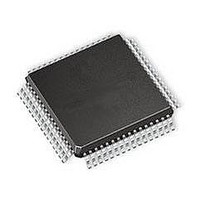
ATMEGA64A-MNR Atmel, ATMEGA64A-MNR Datasheet - Page 163

ATMEGA64A-MNR
Manufacturer Part Number
ATMEGA64A-MNR
Description
IC MCU AVR 64K FLASH 8QFN
Manufacturer
Atmel
Series
AVR® ATmegar
Datasheet
1.ATMEGA64A-AU.pdf
(392 pages)
Specifications of ATMEGA64A-MNR
Core Processor
AVR
Core Size
8-Bit
Speed
16MHz
Connectivity
I²C, SPI, UART/USART
Peripherals
Brown-out Detect/Reset, POR, PWM, WDT
Number Of I /o
53
Program Memory Size
64KB (32K x 16)
Program Memory Type
FLASH
Eeprom Size
2K x 8
Ram Size
4K x 8
Voltage - Supply (vcc/vdd)
2.7 V ~ 5.5 V
Data Converters
A/D 8x10b
Oscillator Type
Internal
Operating Temperature
-40°C ~ 85°C
Package / Case
*
Core
AVR8
Data Bus Width
8 bit
Data Ram Size
2 KB
Interface Type
SPI, UART, I2C
Maximum Clock Frequency
16 MHz
Number Of Programmable I/os
53
Operating Supply Voltage
2.7 V to 5.5 V
Maximum Operating Temperature
+ 105 C
Mounting Style
SMD/SMT
Operating Temperature Range
- 40 C to + 85 C
Processor To Be Evaluated
ATMEGA64A
Lead Free Status / RoHS Status
Lead free / RoHS Compliant
- Current page: 163 of 392
- Download datasheet (8Mb)
18.2.1
8160C–AVR–07/09
Timing Example
When the modulator is enabled the type of modulation (logical AND or OR) can be selected by
the PORTB7 Register. Note that the DDRB7 controls the direction of the port independent of the
COMnx1:0 bit setting.
Figure 18-2
ate in fast PWM mode (non-inverted) and Timer/Counter2 uses CTC waveform mode with toggle
Compare Output mode (COMnx1:0 = 1).
Figure 18-2. Output Compare Modulator, Timing Diagram
In this example, Timer/Counter2 provides the carrier, while the modulating signal is generated
by the Output Compare unit C of the Timer/Counter1.The resolution of the PWM signal (OC1C)
is reduced by the modulation. The reduction factor is equal to the number of system clock cycles
of one period of the carrier (OC2). In this example the resolution is reduced by a factor of two.
The reason for the reduction is illustrated in
PB7 output when PORTB7 equals zero. The period 2 high time is one cycle longer than the
period three high time, but the result on the PB7 output is equal in both periods.
( From Waveform Generator )
( From Waveform Generator )
COM21
COM20
COM1C1
COM1C0
(FPWM Mode)
(PORTB7 = 0)
(PORTB7 = 1)
(CTC Mode)
(Period)
illustrates the modulator in action. In this example the Timer/Counter1 is set to oper-
OC1C
clk
OC2
PB7
PB7
I/O
PORTB7
D
D
D
OC1C
OC2
Q
Q
Q
1
DATA BUS
Figure 18-2
Modulator
0
1
2
at the second and third period of the
DDRB7
D
Q
1
0
ATmega64A
3
Vcc
OC2 / PB7
OC1C /
Pin
163
Related parts for ATMEGA64A-MNR
Image
Part Number
Description
Manufacturer
Datasheet
Request
R

Part Number:
Description:
Manufacturer:
Atmel Corporation
Datasheet:

Part Number:
Description:
Manufacturer:
ATMEL Corporation
Datasheet:

Part Number:
Description:
Manufacturer:
ATMEL Corporation
Datasheet:

Part Number:
Description:
IC AVR MCU 64K 16MHZ 5V 64TQFP
Manufacturer:
Atmel
Datasheet:

Part Number:
Description:
IC AVR MCU 64K 16MHZ 5V 64-QFN
Manufacturer:
Atmel
Datasheet:

Part Number:
Description:
IC AVR MCU 64K 16MHZ COM 64-TQFP
Manufacturer:
Atmel
Datasheet:

Part Number:
Description:
IC AVR MCU 64K 16MHZ IND 64-TQFP
Manufacturer:
Atmel
Datasheet:

Part Number:
Description:
IC AVR MCU 64K 16MHZ COM 64-QFN
Manufacturer:
Atmel
Datasheet:

Part Number:
Description:
MCU AVR 64KB FLASH 16MHZ 64TQFP
Manufacturer:
Atmel
Datasheet:

Part Number:
Description:
MCU AVR 64KB FLASH 16MHZ 64QFN
Manufacturer:
Atmel
Datasheet:

Part Number:
Description:
IC AVR MCU 64K 16MHZ IND 64-QFN
Manufacturer:
Atmel
Datasheet:

Part Number:
Description:
IC MCU AVR 64K 5V 16MHZ 64-TQFP
Manufacturer:
Atmel
Datasheet:

Part Number:
Description:
IC MCU AVR 64K 5V 16MHZ 64-QFN
Manufacturer:
Atmel
Datasheet:

Part Number:
Description:
MCU 8-Bit ATmega AVR RISC 64KB Flash 5V 64-Pin TQFP T/R
Manufacturer:
Atmel
Datasheet:


