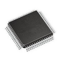
ATMEGA64A-MNR Atmel, ATMEGA64A-MNR Datasheet - Page 129

ATMEGA64A-MNR
Manufacturer Part Number
ATMEGA64A-MNR
Description
IC MCU AVR 64K FLASH 8QFN
Manufacturer
Atmel
Series
AVR® ATmegar
Datasheet
1.ATMEGA64A-AU.pdf
(392 pages)
Specifications of ATMEGA64A-MNR
Core Processor
AVR
Core Size
8-Bit
Speed
16MHz
Connectivity
I²C, SPI, UART/USART
Peripherals
Brown-out Detect/Reset, POR, PWM, WDT
Number Of I /o
53
Program Memory Size
64KB (32K x 16)
Program Memory Type
FLASH
Eeprom Size
2K x 8
Ram Size
4K x 8
Voltage - Supply (vcc/vdd)
2.7 V ~ 5.5 V
Data Converters
A/D 8x10b
Oscillator Type
Internal
Operating Temperature
-40°C ~ 85°C
Package / Case
*
Core
AVR8
Data Bus Width
8 bit
Data Ram Size
2 KB
Interface Type
SPI, UART, I2C
Maximum Clock Frequency
16 MHz
Number Of Programmable I/os
53
Operating Supply Voltage
2.7 V to 5.5 V
Maximum Operating Temperature
+ 105 C
Mounting Style
SMD/SMT
Operating Temperature Range
- 40 C to + 85 C
Processor To Be Evaluated
ATMEGA64A
Lead Free Status / RoHS Status
Lead free / RoHS Compliant
- Current page: 129 of 392
- Download datasheet (8Mb)
8160C–AVR–07/09
The PWM resolution for the phase and frequency correct PWM mode can be defined by either
ICRn or OCRnA. The minimum resolution allowed is 2-bit (ICRn or OCRnA set to 0x0003), and
the maximum resolution is 16-bit (ICRn or OCRnA set to MAX). The PWM resolution in bits can
be calculated using the following equation:
In phase and frequency correct PWM mode the counter is incremented until the counter value
matches either the value in ICRn (WGMn3:0 = 8), or the value in OCRnA (WGMn3:0 = 9). The
counter has then reached the TOP and changes the count direction. The TCNTn value will be
equal to TOP for one timer clock cycle. The timing diagram for the phase correct and frequency
correct PWM mode is shown on
PWM mode when OCRnA or ICRn is used to define TOP. The TCNTn value is in the timing dia-
gram shown as a histogram for illustrating the dual-slope operation. The diagram includes non-
inverted and inverted PWM outputs. The small horizontal line marks on the TCNTn slopes repre-
sent Compare Matches between OCRnx and TCNTn. The OCnx interrupt flag will be set when a
Compare Match occurs.
Figure 15-9. Phase and Frequency Correct PWM Mode, Timing Diagram
The Timer/Counter Overflow Flag (TOVn) is set at the same timer clock cycle as the OCRnx
Registers are updated with the double buffer value (at BOTTOM). When either OCRnA or ICRn
is used for defining the TOP value, the OCnA or ICFn flag set when TCNTn has reached TOP.
The interrupt flags can then be used to generate an interrupt each time the counter reaches the
TOP or BOTTOM value.
When changing the TOP value the program must ensure that the new TOP value is higher or
equal to the value of all of the compare registers. If the TOP value is lower than any of the com-
pare registers, a Compare Match will never occur between the TCNTn and the OCRnx.
As
cal in all periods. Since the OCRnx registers are updated at BOTTOM, the length of the rising
and the falling slopes will always be equal. This gives symmetrical output pulses and is therefore
frequency correct.
Figure 15-9
TCNTn
OCnx
OCnx
Period
shows the output generated is, in contrast to the phase correct mode, symmetri-
1
Figure
R
PFCPWM
2
15-9. The figure shows phase and frequency correct
=
log
---------------------------------- -
3
(
log
TOP
2 ( )
+
1
)
4
ATmega64A
OCnA Interrupt Flag Set
or ICFn Interrupt Flag Set
(Interrupt on TOP)
OCRnx / TOP Update and
TOVn Interrupt Flag Set
(Interrupt on Bottom)
(COMnx1:0 = 2)
(COMnx1:0 = 3)
129
Related parts for ATMEGA64A-MNR
Image
Part Number
Description
Manufacturer
Datasheet
Request
R

Part Number:
Description:
Manufacturer:
Atmel Corporation
Datasheet:

Part Number:
Description:
Manufacturer:
ATMEL Corporation
Datasheet:

Part Number:
Description:
Manufacturer:
ATMEL Corporation
Datasheet:

Part Number:
Description:
IC AVR MCU 64K 16MHZ 5V 64TQFP
Manufacturer:
Atmel
Datasheet:

Part Number:
Description:
IC AVR MCU 64K 16MHZ 5V 64-QFN
Manufacturer:
Atmel
Datasheet:

Part Number:
Description:
IC AVR MCU 64K 16MHZ COM 64-TQFP
Manufacturer:
Atmel
Datasheet:

Part Number:
Description:
IC AVR MCU 64K 16MHZ IND 64-TQFP
Manufacturer:
Atmel
Datasheet:

Part Number:
Description:
IC AVR MCU 64K 16MHZ COM 64-QFN
Manufacturer:
Atmel
Datasheet:

Part Number:
Description:
MCU AVR 64KB FLASH 16MHZ 64TQFP
Manufacturer:
Atmel
Datasheet:

Part Number:
Description:
MCU AVR 64KB FLASH 16MHZ 64QFN
Manufacturer:
Atmel
Datasheet:

Part Number:
Description:
IC AVR MCU 64K 16MHZ IND 64-QFN
Manufacturer:
Atmel
Datasheet:

Part Number:
Description:
IC MCU AVR 64K 5V 16MHZ 64-TQFP
Manufacturer:
Atmel
Datasheet:

Part Number:
Description:
IC MCU AVR 64K 5V 16MHZ 64-QFN
Manufacturer:
Atmel
Datasheet:

Part Number:
Description:
MCU 8-Bit ATmega AVR RISC 64KB Flash 5V 64-Pin TQFP T/R
Manufacturer:
Atmel
Datasheet:


