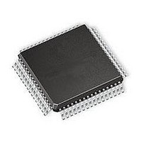
ATMEGA64A-MNR Atmel, ATMEGA64A-MNR Datasheet - Page 262

ATMEGA64A-MNR
Manufacturer Part Number
ATMEGA64A-MNR
Description
IC MCU AVR 64K FLASH 8QFN
Manufacturer
Atmel
Series
AVR® ATmegar
Datasheet
1.ATMEGA64A-AU.pdf
(392 pages)
Specifications of ATMEGA64A-MNR
Core Processor
AVR
Core Size
8-Bit
Speed
16MHz
Connectivity
I²C, SPI, UART/USART
Peripherals
Brown-out Detect/Reset, POR, PWM, WDT
Number Of I /o
53
Program Memory Size
64KB (32K x 16)
Program Memory Type
FLASH
Eeprom Size
2K x 8
Ram Size
4K x 8
Voltage - Supply (vcc/vdd)
2.7 V ~ 5.5 V
Data Converters
A/D 8x10b
Oscillator Type
Internal
Operating Temperature
-40°C ~ 85°C
Package / Case
*
Core
AVR8
Data Bus Width
8 bit
Data Ram Size
2 KB
Interface Type
SPI, UART, I2C
Maximum Clock Frequency
16 MHz
Number Of Programmable I/os
53
Operating Supply Voltage
2.7 V to 5.5 V
Maximum Operating Temperature
+ 105 C
Mounting Style
SMD/SMT
Operating Temperature Range
- 40 C to + 85 C
Processor To Be Evaluated
ATMEGA64A
Lead Free Status / RoHS Status
Lead free / RoHS Compliant
- Current page: 262 of 392
- Download datasheet (8Mb)
25.4.2
25.4.3
25.4.4
25.4.5
25.5
25.5.1
8160C–AVR–07/09
Boundary-scan Chain
IDCODE; 0x1
SAMPLE_PRELOAD; 0x2
AVR_RESET; 0xC
BYPASS; 0xF
Scanning the Digital Port Pins
Optional JTAG instruction selecting the 32-bit ID-Register as data register. The ID-Register con-
sists of a version number, a device number and the manufacturer code chosen by JEDEC. This
is the default instruction after Power-up.
The active states are:
Mandatory JTAG instruction for taking a snap-shot of the input/output pins without affecting the
system operation, and pre-loading the output latches. However, the output latches are not con-
nected to the pins. The Boundary-scan Chain is selected as data register.
The active states are:
The AVR specific public JTAG instruction for forcing the AVR device into the Reset mode or
releasing the JTAG Reset source. The TAP controller is not reset by this instruction. The one bit
Reset Register is selected as data register. Note that the reset will be active as long as there is
a logic “one” in the Reset Chain. The output from this chain is not latched.
The active states are:
Mandatory JTAG instruction selecting the Bypass Register for Data Register.
The active states are:
The Boundary-scan Chain has the capability of driving and observing the logic levels on the dig-
ital I/O pins, as well as the boundary between digital and analog logic for analog circuitry having
Off-chip connection.
Figure 25-3
cell consists of a standard Boundary-scan cell for the Pull-up Enable – PUExn – function, and a
bi-directional pin cell that combines the three signals, Output Control – OCxn, Output Data –
ODxn, and Input Data – IDxn, into only a two-stage Shift Register. The port and pin indexes are
not used in the following description.
• Capture-DR: Data in the IDCODE Register is sampled into the Boundary-scan Chain.
• Shift-DR: The IDCODE scan chain is shifted by the TCK input.
• Capture-DR: Data on the external pins are sampled into the Boundary-scan Chain.
• Shift-DR: The Boundary-scan Chain is shifted by the TCK input.
• Update-DR: Data from the Boundary-scan Chain is applied to the output latches. However,
• Shift-DR: The Reset Register is shifted by the TCK input.
• Capture-DR: Loads a logic “0” into the Bypass Register.
• Shift-DR: The Bypass Register cell between TDI and TDO is shifted.
the output latches are not connected to the pins.
shows the Boundary-scan Cell for a bi-directional port pin with pull-up function. The
ATmega64A
262
Related parts for ATMEGA64A-MNR
Image
Part Number
Description
Manufacturer
Datasheet
Request
R

Part Number:
Description:
Manufacturer:
Atmel Corporation
Datasheet:

Part Number:
Description:
Manufacturer:
ATMEL Corporation
Datasheet:

Part Number:
Description:
Manufacturer:
ATMEL Corporation
Datasheet:

Part Number:
Description:
IC AVR MCU 64K 16MHZ 5V 64TQFP
Manufacturer:
Atmel
Datasheet:

Part Number:
Description:
IC AVR MCU 64K 16MHZ 5V 64-QFN
Manufacturer:
Atmel
Datasheet:

Part Number:
Description:
IC AVR MCU 64K 16MHZ COM 64-TQFP
Manufacturer:
Atmel
Datasheet:

Part Number:
Description:
IC AVR MCU 64K 16MHZ IND 64-TQFP
Manufacturer:
Atmel
Datasheet:

Part Number:
Description:
IC AVR MCU 64K 16MHZ COM 64-QFN
Manufacturer:
Atmel
Datasheet:

Part Number:
Description:
MCU AVR 64KB FLASH 16MHZ 64TQFP
Manufacturer:
Atmel
Datasheet:

Part Number:
Description:
MCU AVR 64KB FLASH 16MHZ 64QFN
Manufacturer:
Atmel
Datasheet:

Part Number:
Description:
IC AVR MCU 64K 16MHZ IND 64-QFN
Manufacturer:
Atmel
Datasheet:

Part Number:
Description:
IC MCU AVR 64K 5V 16MHZ 64-TQFP
Manufacturer:
Atmel
Datasheet:

Part Number:
Description:
IC MCU AVR 64K 5V 16MHZ 64-QFN
Manufacturer:
Atmel
Datasheet:

Part Number:
Description:
MCU 8-Bit ATmega AVR RISC 64KB Flash 5V 64-Pin TQFP T/R
Manufacturer:
Atmel
Datasheet:


