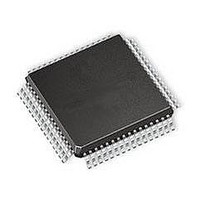
ATMEGA64A-MNR Atmel, ATMEGA64A-MNR Datasheet - Page 109

ATMEGA64A-MNR
Manufacturer Part Number
ATMEGA64A-MNR
Description
IC MCU AVR 64K FLASH 8QFN
Manufacturer
Atmel
Series
AVR® ATmegar
Datasheet
1.ATMEGA64A-AU.pdf
(392 pages)
Specifications of ATMEGA64A-MNR
Core Processor
AVR
Core Size
8-Bit
Speed
16MHz
Connectivity
I²C, SPI, UART/USART
Peripherals
Brown-out Detect/Reset, POR, PWM, WDT
Number Of I /o
53
Program Memory Size
64KB (32K x 16)
Program Memory Type
FLASH
Eeprom Size
2K x 8
Ram Size
4K x 8
Voltage - Supply (vcc/vdd)
2.7 V ~ 5.5 V
Data Converters
A/D 8x10b
Oscillator Type
Internal
Operating Temperature
-40°C ~ 85°C
Package / Case
*
Core
AVR8
Data Bus Width
8 bit
Data Ram Size
2 KB
Interface Type
SPI, UART, I2C
Maximum Clock Frequency
16 MHz
Number Of Programmable I/os
53
Operating Supply Voltage
2.7 V to 5.5 V
Maximum Operating Temperature
+ 105 C
Mounting Style
SMD/SMT
Operating Temperature Range
- 40 C to + 85 C
Processor To Be Evaluated
ATMEGA64A
Lead Free Status / RoHS Status
Lead free / RoHS Compliant
- Current page: 109 of 392
- Download datasheet (8Mb)
14.11.5
14.11.6
8160C–AVR–07/09
TIMSK – Timer/Counter Interrupt Mask Register
TIFR – Timer/Counter Interrupt Flag Register
• Bit 2 – TCN0UB: Timer/Counter0 Update Busy
When Timer/Counter0 operates asynchronously and TCNT0 is written, this bit becomes set.
When TCNT0 has been updated from the temporary storage register, this bit is cleared by hard-
ware. A logical zero in this bit indicates that TCNT0 is ready to be updated with a new value.
• Bit 1 – OCR0UB: Output Compare Register0 Update Busy
When Timer/Counter0 operates asynchronously and OCR0 is written, this bit becomes set.
When OCR0 has been updated from the temporary storage register, this bit is cleared by hard-
ware. A logical zero in this bit indicates that OCR0 is ready to be updated with a new value.
• Bit 0 – TCR0UB: Timer/Counter Control Register0 Update Busy
When Timer/Counter0 operates asynchronously and TCCR0 is written, this bit becomes set.
When TCCR0 has been updated from the temporary storage register, this bit is cleared by hard-
ware. A logical zero in this bit indicates that TCCR0 is ready to be updated with a new value.
If a write is performed to any of the three Timer/Counter0 registers while its update busy flag is
set, the updated value might get corrupted and cause an unintentional interrupt to occur.
The mechanisms for reading TCNT0, OCR0, and TCCR0 are different. When reading TCNT0,
the actual timer value is read. When reading OCR0 or TCCR0, the value in the temporary stor-
age register is read.
• Bit 1 – OCIE0: Timer/Counter0 Output Compare Match Interrupt Enable
When the OCIE0 bit is written to one, and the I-bit in the Status Register is set (one), the
Timer/Counter0 Compare Match interrupt is enabled. The corresponding interrupt is executed if
a Compare Match in Timer/Counter0 occurs, i.e., when the OCF0 bit is set in the Timer/Counter
Interrupt Flag Register – TIFR.
• Bit 0 – TOIE0: Timer/Counter0 Overflow Interrupt Enable
When the TOIE0 bit is written to one, and the I-bit in the Status Register is set (one), the
Timer/Counter0 Overflow interrupt is enabled. The corresponding interrupt is executed if an
overflow in Timer/Counter0 occurs, i.e., when the TOV0 bit is set in the Timer/Counter Interrupt
Flag Register – TIFR.
• Bit 1 – OCF0: Output Compare Flag 0
The OCF0 bit is set (one) when a Compare Match occurs between the Timer/Counter0 and the
data in OCR0 – Output Compare Register0. OCF0 is cleared by hardware when executing the
corresponding interrupt handling vector. Alternatively, OCF0 is cleared by writing a logic one to
Bit
0x37 (0x57)
Read/Write
Initial Value
Bit
0x36 (0x56)
Read/Write
Initial Value
OCF2
R/W
7
0
OCIE2
R/W
7
0
TOV2
R/W
6
0
TOIE2
R/W
6
0
ICF1
R/W
TICIE1
5
0
R/W
5
0
OCF1A
OCIE1A
R/W
4
0
R/W
4
0
OCF1B
OCIE1B
R/W
R/W
3
0
3
0
TOV1
R/W
TOIE1
R/W
2
0
2
0
OCF0
OCIE0
R/W
R/W
1
0
1
0
ATmega64A
TOV0
TOIE0
R/W
R/W
0
0
0
0
TIMSK
TIFR
109
Related parts for ATMEGA64A-MNR
Image
Part Number
Description
Manufacturer
Datasheet
Request
R

Part Number:
Description:
Manufacturer:
Atmel Corporation
Datasheet:

Part Number:
Description:
Manufacturer:
ATMEL Corporation
Datasheet:

Part Number:
Description:
Manufacturer:
ATMEL Corporation
Datasheet:

Part Number:
Description:
IC AVR MCU 64K 16MHZ 5V 64TQFP
Manufacturer:
Atmel
Datasheet:

Part Number:
Description:
IC AVR MCU 64K 16MHZ 5V 64-QFN
Manufacturer:
Atmel
Datasheet:

Part Number:
Description:
IC AVR MCU 64K 16MHZ COM 64-TQFP
Manufacturer:
Atmel
Datasheet:

Part Number:
Description:
IC AVR MCU 64K 16MHZ IND 64-TQFP
Manufacturer:
Atmel
Datasheet:

Part Number:
Description:
IC AVR MCU 64K 16MHZ COM 64-QFN
Manufacturer:
Atmel
Datasheet:

Part Number:
Description:
MCU AVR 64KB FLASH 16MHZ 64TQFP
Manufacturer:
Atmel
Datasheet:

Part Number:
Description:
MCU AVR 64KB FLASH 16MHZ 64QFN
Manufacturer:
Atmel
Datasheet:

Part Number:
Description:
IC AVR MCU 64K 16MHZ IND 64-QFN
Manufacturer:
Atmel
Datasheet:

Part Number:
Description:
IC MCU AVR 64K 5V 16MHZ 64-TQFP
Manufacturer:
Atmel
Datasheet:

Part Number:
Description:
IC MCU AVR 64K 5V 16MHZ 64-QFN
Manufacturer:
Atmel
Datasheet:

Part Number:
Description:
MCU 8-Bit ATmega AVR RISC 64KB Flash 5V 64-Pin TQFP T/R
Manufacturer:
Atmel
Datasheet:


