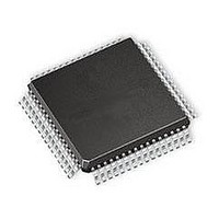
ATMEGA64A-MNR Atmel, ATMEGA64A-MNR Datasheet - Page 188

ATMEGA64A-MNR
Manufacturer Part Number
ATMEGA64A-MNR
Description
IC MCU AVR 64K FLASH 8QFN
Manufacturer
Atmel
Series
AVR® ATmegar
Datasheet
1.ATMEGA64A-AU.pdf
(392 pages)
Specifications of ATMEGA64A-MNR
Core Processor
AVR
Core Size
8-Bit
Speed
16MHz
Connectivity
I²C, SPI, UART/USART
Peripherals
Brown-out Detect/Reset, POR, PWM, WDT
Number Of I /o
53
Program Memory Size
64KB (32K x 16)
Program Memory Type
FLASH
Eeprom Size
2K x 8
Ram Size
4K x 8
Voltage - Supply (vcc/vdd)
2.7 V ~ 5.5 V
Data Converters
A/D 8x10b
Oscillator Type
Internal
Operating Temperature
-40°C ~ 85°C
Package / Case
*
Core
AVR8
Data Bus Width
8 bit
Data Ram Size
2 KB
Interface Type
SPI, UART, I2C
Maximum Clock Frequency
16 MHz
Number Of Programmable I/os
53
Operating Supply Voltage
2.7 V to 5.5 V
Maximum Operating Temperature
+ 105 C
Mounting Style
SMD/SMT
Operating Temperature Range
- 40 C to + 85 C
Processor To Be Evaluated
ATMEGA64A
Lead Free Status / RoHS Status
Lead free / RoHS Compliant
- Current page: 188 of 392
- Download datasheet (8Mb)
20.8.2
8160C–AVR–07/09
Asynchronous Data Recovery
Figure 20-5. Start Bit Sampling
When the Clock Recovery logic detects a high (idle) to low (start) transition on the RxD line, the
start bit detection sequence is initiated. Let sample 1 denote the first zero-sample as shown in
the figure. The Clock Recovery logic then uses samples 8, 9 and 10 for Normal mode, and sam-
ples 4, 5 and 6 for Double Speed mode (indicated with sample numbers inside boxes on the
figure), to decide if a valid start bit is received. If two or more of these three samples have logical
high levels (the majority wins), the start bit is rejected as a noise spike and the Receiver starts
looking for the next high to low-transition. If however, a valid start bit is detected, the clock recov-
ery logic is synchronized and the data recovery can begin. The synchronization process is
repeated for each start bit.
When the receiver clock is synchronized to the start bit, the data recovery can begin. The data
recovery unit uses a state machine that has 16 states for each bit in Normal mode and eight
states for each bit in Double Speed mode.
the parity bit. Each of the samples is given a number that is equal to the state of the recovery
unit.
Figure 20-6. Sampling of Data and Parity Bit
The decision of the logic level of the received bit is taken by doing a majority voting of the logic
value to the three samples in the center of the received bit. The center samples are emphasized
on the figure by having the sample number inside boxes. The majority voting process is done as
follows: If two or all three samples have high levels, the received bit is registered to be a logic 1.
If two or all three samples have low levels, the received bit is registered to be a logic 0. This
majority voting process acts as a low pass filter for the incoming signal on the RxD pin. The
recovery process is then repeated until a complete frame is received. Including the first stop bit.
Note that the receiver only uses the first stop bit of a frame.
the stop bit and the earliest possible beginning of the start bit of the next frame.
(U2X = 0)
(U2X = 1)
(U2X = 0)
(U2X = 1)
Sample
Sample
Sample
Sample
RxD
RxD
0
0
IDLE
0
1
1
1
1
2
2
3
2
3
2
4
4
5
3
5
3
6
6
Figure 20-6
7
4
7
4
8
8
START
BIT n
9
5
9
5
10
10
shows the sampling of the data bits and
11
11
6
6
Figure 20-7
12
12
13
13
7
7
14
14
ATmega64A
shows the sampling of
15
15
8
8
16
16
1
1
1
1
2
BIT 0
3
2
188
Related parts for ATMEGA64A-MNR
Image
Part Number
Description
Manufacturer
Datasheet
Request
R

Part Number:
Description:
Manufacturer:
Atmel Corporation
Datasheet:

Part Number:
Description:
Manufacturer:
ATMEL Corporation
Datasheet:

Part Number:
Description:
Manufacturer:
ATMEL Corporation
Datasheet:

Part Number:
Description:
IC AVR MCU 64K 16MHZ 5V 64TQFP
Manufacturer:
Atmel
Datasheet:

Part Number:
Description:
IC AVR MCU 64K 16MHZ 5V 64-QFN
Manufacturer:
Atmel
Datasheet:

Part Number:
Description:
IC AVR MCU 64K 16MHZ COM 64-TQFP
Manufacturer:
Atmel
Datasheet:

Part Number:
Description:
IC AVR MCU 64K 16MHZ IND 64-TQFP
Manufacturer:
Atmel
Datasheet:

Part Number:
Description:
IC AVR MCU 64K 16MHZ COM 64-QFN
Manufacturer:
Atmel
Datasheet:

Part Number:
Description:
MCU AVR 64KB FLASH 16MHZ 64TQFP
Manufacturer:
Atmel
Datasheet:

Part Number:
Description:
MCU AVR 64KB FLASH 16MHZ 64QFN
Manufacturer:
Atmel
Datasheet:

Part Number:
Description:
IC AVR MCU 64K 16MHZ IND 64-QFN
Manufacturer:
Atmel
Datasheet:

Part Number:
Description:
IC MCU AVR 64K 5V 16MHZ 64-TQFP
Manufacturer:
Atmel
Datasheet:

Part Number:
Description:
IC MCU AVR 64K 5V 16MHZ 64-QFN
Manufacturer:
Atmel
Datasheet:

Part Number:
Description:
MCU 8-Bit ATmega AVR RISC 64KB Flash 5V 64-Pin TQFP T/R
Manufacturer:
Atmel
Datasheet:


