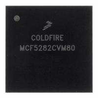
MCF5282CVM80 Freescale Semiconductor, MCF5282CVM80 Datasheet - Page 667

MCF5282CVM80
Manufacturer Part Number
MCF5282CVM80
Description
IC MPU 512K 80MHZ 256-MAPBGA
Manufacturer
Freescale Semiconductor
Series
MCF528xr
Datasheet
1.MCF5216CVM66J.pdf
(766 pages)
Specifications of MCF5282CVM80
Core Processor
Coldfire V2
Core Size
32-Bit
Speed
80MHz
Connectivity
CAN, EBI/EMI, Ethernet, I²C, SPI, UART/USART
Peripherals
DMA, LVD, POR, PWM, WDT
Number Of I /o
150
Program Memory Size
512KB (512K x 8)
Program Memory Type
FLASH
Ram Size
64K x 8
Voltage - Supply (vcc/vdd)
2.7 V ~ 3.6 V
Data Converters
A/D 8x10b
Oscillator Type
External
Operating Temperature
-40°C ~ 85°C
Package / Case
256-MAPBGA
Controller Family/series
ColdFire
Ram Memory Size
64KB
Embedded Interface Type
CAN, I2C, SPI, UART
No. Of Pwm Channels
8
Digital Ic Case Style
MAPBGA
Rohs Compliant
Yes
Lead Free Status / RoHS Status
Lead free / RoHS Compliant
Eeprom Size
-
Available stocks
Company
Part Number
Manufacturer
Quantity
Price
Company:
Part Number:
MCF5282CVM80
Manufacturer:
FREESCALE
Quantity:
1 831
Company:
Part Number:
MCF5282CVM80
Manufacturer:
Freescale Semiconductor
Quantity:
10 000
Company:
Part Number:
MCF5282CVM80J
Manufacturer:
Freescale Semiconductor
Quantity:
10 000
- Current page: 667 of 766
- Download datasheet (9Mb)
When one module is selected, the inputs into the other module are disabled or forced to a known logic level
as shown in
31.3.1.2 TCLK — Test Clock Input
The TCLK pin is a dedicated JTAG clock input to synchronize the test logic. Pulses on TCLK shift data
and instructions into the TDI pin on the rising edge and out of the TDO pin on the falling edge. TCLK is
independent of the processor clock. The TCLK pin has an internal pull-up resistor and holding TCLK high
or low for an indefinite period does not cause JTAG test logic to lose state information.
31.3.1.3 TMS/BKPT — Test Mode Select / Breakpoint
The TMS pin is the test mode select input that sequences the TAP state machine. TMS is sampled on the
rising edge of TCLK. The TMS pin has an internal pull-up resistor.
The BKPT pin is used to request an external breakpoint. Assertion of BKPT puts the processor into a halted
state after the current instruction completes.
31.3.1.4 TDI/DSI — Test Data Input / Development Serial Input
The TDI pin is the LSB-first data and instruction input. TDI is sampled on the rising edge of TCLK. The
TDI pin has an internal pull-up resistor.
The DSI pin provides data input for the debug module serial communication port.
31.3.1.5 TRST/DSCLK — Test Reset / Development Serial Clock
The TRST pin is an active low asynchronous reset input with an internal pull-up resistor that forces the
TAP controller to the test-logic-reset state.
Freescale Semiconductor
Table
The JTAG_EN does not support dynamic switching between JTAG and
BDM modes.
Module selected
Pin Function
31-3, in order to disable the corresponding module.
MCF5282 and MCF5216 ColdFire Microcontroller User’s Manual, Rev. 3
Disabling JTAG
Disabling BDM
Table 31-3. Signal State to the Disable Module
Table 31-2. Pin Function Selected
DSCLK
BKPT
BDM
DSO
DSI
—
JTAG_EN = 0
TRST = 0
TMS = 1
NOTE
—
TCLK
TRST
JTAG
TMS
TDO
TDI
Disable DSCLK
JTAG_EN = 1
BKPT = 1
DSI = 0
—
IEEE 1149.1 Test Access Port (JTAG)
DSCLK
BKPT
TCLK
DSO
DSI
—
31-3
Related parts for MCF5282CVM80
Image
Part Number
Description
Manufacturer
Datasheet
Request
R
Part Number:
Description:
Mcf5282 And Mcf5216 Coldfire Microcontroller User�s Manual
Manufacturer:
Freescale Semiconductor, Inc
Datasheet:
Part Number:
Description:
Manufacturer:
Freescale Semiconductor, Inc
Datasheet:
Part Number:
Description:
Manufacturer:
Freescale Semiconductor, Inc
Datasheet:
Part Number:
Description:
Manufacturer:
Freescale Semiconductor, Inc
Datasheet:
Part Number:
Description:
Manufacturer:
Freescale Semiconductor, Inc
Datasheet:
Part Number:
Description:
Manufacturer:
Freescale Semiconductor, Inc
Datasheet:
Part Number:
Description:
Manufacturer:
Freescale Semiconductor, Inc
Datasheet:
Part Number:
Description:
Manufacturer:
Freescale Semiconductor, Inc
Datasheet:
Part Number:
Description:
Manufacturer:
Freescale Semiconductor, Inc
Datasheet:
Part Number:
Description:
Manufacturer:
Freescale Semiconductor, Inc
Datasheet:
Part Number:
Description:
Manufacturer:
Freescale Semiconductor, Inc
Datasheet:
Part Number:
Description:
Manufacturer:
Freescale Semiconductor, Inc
Datasheet:
Part Number:
Description:
Manufacturer:
Freescale Semiconductor, Inc
Datasheet:
Part Number:
Description:
Manufacturer:
Freescale Semiconductor, Inc
Datasheet:
Part Number:
Description:
Manufacturer:
Freescale Semiconductor, Inc
Datasheet:


