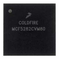
MCF5282CVM80 Freescale Semiconductor, MCF5282CVM80 Datasheet - Page 416

MCF5282CVM80
Manufacturer Part Number
MCF5282CVM80
Description
IC MPU 512K 80MHZ 256-MAPBGA
Manufacturer
Freescale Semiconductor
Series
MCF528xr
Datasheet
1.MCF5216CVM66J.pdf
(766 pages)
Specifications of MCF5282CVM80
Core Processor
Coldfire V2
Core Size
32-Bit
Speed
80MHz
Connectivity
CAN, EBI/EMI, Ethernet, I²C, SPI, UART/USART
Peripherals
DMA, LVD, POR, PWM, WDT
Number Of I /o
150
Program Memory Size
512KB (512K x 8)
Program Memory Type
FLASH
Ram Size
64K x 8
Voltage - Supply (vcc/vdd)
2.7 V ~ 3.6 V
Data Converters
A/D 8x10b
Oscillator Type
External
Operating Temperature
-40°C ~ 85°C
Package / Case
256-MAPBGA
Controller Family/series
ColdFire
Ram Memory Size
64KB
Embedded Interface Type
CAN, I2C, SPI, UART
No. Of Pwm Channels
8
Digital Ic Case Style
MAPBGA
Rohs Compliant
Yes
Lead Free Status / RoHS Status
Lead free / RoHS Compliant
Eeprom Size
-
Available stocks
Company
Part Number
Manufacturer
Quantity
Price
Company:
Part Number:
MCF5282CVM80
Manufacturer:
FREESCALE
Quantity:
1 831
Company:
Part Number:
MCF5282CVM80
Manufacturer:
Freescale Semiconductor
Quantity:
10 000
Company:
Part Number:
MCF5282CVM80J
Manufacturer:
Freescale Semiconductor
Quantity:
10 000
- Current page: 416 of 766
- Download datasheet (9Mb)
Queued Serial Peripheral Interface (QSPI)
the least significant bits of the RAM. Unused bits in a receive queue entry are set to zero upon completion
of the individual queue entry. Receive RAM is not writeable.
QWR[CPTQP] shows which queue entries have been executed. The user can query this field to determine
which locations in receive RAM contain valid data.
22.4.1.2
Data to be transmitted by the QSPI is stored in the transmit RAM segment located at addresses 0x0 to 0xF.
The user normally writes 1 word into this segment for each queue command to be executed. The user
cannot read data in the transmit RAM.
Outbound data must be written to transmit RAM in a right-justified format. The unused bits are ignored.
The QSPI copies the data to its data serializer (shift register) for transmission. The data is transmitted most
significant bit first and remains in transmit RAM until overwritten by the user.
22.4.1.3
The CPU writes one byte of control information to this segment for each QSPI command to be executed.
Command RAM, referred to as QCR0–15, is write-only memory from a user’s perspective.
Command RAM consists of 16 bytes, each divided into two fields. The peripheral chip select field controls
the QSPI_CS signal levels for the transfer. The command control field provides transfer options.
A maximum of 16 commands can be in the queue. Queue execution proceeds from the address in
QWR[NEWQP] through the address in QWR[ENDQP].
The QSPI executes a queue of commands defined by the control bits in each command RAM entry that
sequence the following actions:
Before any data transfers begin, control data must be written to the command RAM, and any out-bound
data must be written to the transmit RAM. Also, the queue pointers must be initialized to the first and last
entries in the command queue.
Data transfer is synchronized with the internally generated QSPI_CLK, whose phase and polarity are
controlled by QMR[CPHA] and QMR[CPOL]. These control bits determine which QSPI_CLK edge is
used to drive outgoing data and to latch incoming data.
22.4.2
The maximum QSPI clock frequency is one-fourth the clock frequency of the internal bus clock (f
Baud rate is selected by writing a value from 2–255 into QMR[BAUD]. The QSPI uses a prescaler to
derive the QSPI_CLK rate from the internal bus clock divided by two.
frequency as a function of internal bus clock and baud rate.
A baud rate value of zero turns off the QSPI_CLK.
22-12
•
•
•
Chip-select pins are activated.
Data is transmitted from the transmit RAM and received into the receive RAM.
The synchronous transfer clock QSPI_CLK is generated.
Baud Rate Selection
Transmit RAM
Command RAM
MCF5282 and MCF5216 ColdFire Microcontroller User’s Manual, Rev. 3
Table 22-10
shows the QSPI_CLK
Freescale Semiconductor
sys
).
Related parts for MCF5282CVM80
Image
Part Number
Description
Manufacturer
Datasheet
Request
R
Part Number:
Description:
Mcf5282 And Mcf5216 Coldfire Microcontroller User�s Manual
Manufacturer:
Freescale Semiconductor, Inc
Datasheet:
Part Number:
Description:
Manufacturer:
Freescale Semiconductor, Inc
Datasheet:
Part Number:
Description:
Manufacturer:
Freescale Semiconductor, Inc
Datasheet:
Part Number:
Description:
Manufacturer:
Freescale Semiconductor, Inc
Datasheet:
Part Number:
Description:
Manufacturer:
Freescale Semiconductor, Inc
Datasheet:
Part Number:
Description:
Manufacturer:
Freescale Semiconductor, Inc
Datasheet:
Part Number:
Description:
Manufacturer:
Freescale Semiconductor, Inc
Datasheet:
Part Number:
Description:
Manufacturer:
Freescale Semiconductor, Inc
Datasheet:
Part Number:
Description:
Manufacturer:
Freescale Semiconductor, Inc
Datasheet:
Part Number:
Description:
Manufacturer:
Freescale Semiconductor, Inc
Datasheet:
Part Number:
Description:
Manufacturer:
Freescale Semiconductor, Inc
Datasheet:
Part Number:
Description:
Manufacturer:
Freescale Semiconductor, Inc
Datasheet:
Part Number:
Description:
Manufacturer:
Freescale Semiconductor, Inc
Datasheet:
Part Number:
Description:
Manufacturer:
Freescale Semiconductor, Inc
Datasheet:
Part Number:
Description:
Manufacturer:
Freescale Semiconductor, Inc
Datasheet:


