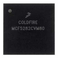
MCF5282CVM80 Freescale Semiconductor, MCF5282CVM80 Datasheet - Page 280

MCF5282CVM80
Manufacturer Part Number
MCF5282CVM80
Description
IC MPU 512K 80MHZ 256-MAPBGA
Manufacturer
Freescale Semiconductor
Series
MCF528xr
Datasheet
1.MCF5216CVM66J.pdf
(766 pages)
Specifications of MCF5282CVM80
Core Processor
Coldfire V2
Core Size
32-Bit
Speed
80MHz
Connectivity
CAN, EBI/EMI, Ethernet, I²C, SPI, UART/USART
Peripherals
DMA, LVD, POR, PWM, WDT
Number Of I /o
150
Program Memory Size
512KB (512K x 8)
Program Memory Type
FLASH
Ram Size
64K x 8
Voltage - Supply (vcc/vdd)
2.7 V ~ 3.6 V
Data Converters
A/D 8x10b
Oscillator Type
External
Operating Temperature
-40°C ~ 85°C
Package / Case
256-MAPBGA
Controller Family/series
ColdFire
Ram Memory Size
64KB
Embedded Interface Type
CAN, I2C, SPI, UART
No. Of Pwm Channels
8
Digital Ic Case Style
MAPBGA
Rohs Compliant
Yes
Lead Free Status / RoHS Status
Lead free / RoHS Compliant
Eeprom Size
-
Available stocks
Company
Part Number
Manufacturer
Quantity
Price
Company:
Part Number:
MCF5282CVM80
Manufacturer:
FREESCALE
Quantity:
1 831
Company:
Part Number:
MCF5282CVM80
Manufacturer:
Freescale Semiconductor
Quantity:
10 000
Company:
Part Number:
MCF5282CVM80J
Manufacturer:
Freescale Semiconductor
Quantity:
10 000
- Current page: 280 of 766
- Download datasheet (9Mb)
Synchronous DRAM Controller Module
15.2.2.3 DRAM Controller Mask Registers (DMR0/DMR1)
The DMRn,
Table 15-6
15-8
31–18
17–9
Bits
6–1
Reset
8
7
0
Field
Addr
R/W
31
Name
BAM
describes DMRn fields.
AMx
WP
—
—
V
Figure
Base address mask. Masks the associated DACRn[BA]. Lets the DRAM controller connect to various
DRAM sizes. Mask bits need not be contiguous (see
0 The associated address bit is used in decoding the DRAM hit to a memory block.
1 The associated address bit is not used in the DRAM hit decode.
Reserved, should be cleared.
Write protect. Determines whether the associated block of DRAM is write protected.
0 Allow write accesses
1 Ignore write accesses. The DRAM controller ignores write accesses to the memory block and an
Reserved, should be cleared.
Address modifier masks. Determine which accesses can occur in a given DRAM block.
0 Allow access type to hit in DRAM
1 Do not allow access type to hit in DRAM
Valid. Cleared at reset to ensure that the DRAM block is not erroneously decoded.
0 Do not decode DRAM accesses.
1 Registers controlling the DRAM block are initialized; DRAM accesses can be decoded.
15-4, includes mask bits for the base address and for address attributes.
address exception occurs. Write accesses to a write-protected DRAM region are compared in the
chip select module for a hit. If no hit occurs, an external bus cycle is generated. If this external bus
cycle is not acknowledged, an access exception occurs.
AM Alternate master
SC
SD
UC
UD
Bit
C/I
MCF5282 and MCF5216 ColdFire Microcontroller User’s Manual, Rev. 3
BAM
CPU space/interrupt acknowledge
Supervisor code
Supervisor data
User code
User data
Figure 15-4. DRAM Controller Mask Registers (DMRn)
Associated Access Type
Table 15-6. DMRn Field Descriptions
IPSBAR + 0x04C (DMR0), 0x054 (DMR1)
18 17
Uninitialized
R/W
Description
—
MOVEC instruction or interrupt acknowledge cycle
DMA master
Any supervisor-only instruction access
Any data fetched during the instruction access
Any user instruction
Any user data
Section 15.3, “SDRAM
9
WP — C/I AM SC SD UC UD V
8
Access Definition
7
6
5
Example.”)
Freescale Semiconductor
4
3
2
1
0
0
Related parts for MCF5282CVM80
Image
Part Number
Description
Manufacturer
Datasheet
Request
R
Part Number:
Description:
Mcf5282 And Mcf5216 Coldfire Microcontroller User�s Manual
Manufacturer:
Freescale Semiconductor, Inc
Datasheet:
Part Number:
Description:
Manufacturer:
Freescale Semiconductor, Inc
Datasheet:
Part Number:
Description:
Manufacturer:
Freescale Semiconductor, Inc
Datasheet:
Part Number:
Description:
Manufacturer:
Freescale Semiconductor, Inc
Datasheet:
Part Number:
Description:
Manufacturer:
Freescale Semiconductor, Inc
Datasheet:
Part Number:
Description:
Manufacturer:
Freescale Semiconductor, Inc
Datasheet:
Part Number:
Description:
Manufacturer:
Freescale Semiconductor, Inc
Datasheet:
Part Number:
Description:
Manufacturer:
Freescale Semiconductor, Inc
Datasheet:
Part Number:
Description:
Manufacturer:
Freescale Semiconductor, Inc
Datasheet:
Part Number:
Description:
Manufacturer:
Freescale Semiconductor, Inc
Datasheet:
Part Number:
Description:
Manufacturer:
Freescale Semiconductor, Inc
Datasheet:
Part Number:
Description:
Manufacturer:
Freescale Semiconductor, Inc
Datasheet:
Part Number:
Description:
Manufacturer:
Freescale Semiconductor, Inc
Datasheet:
Part Number:
Description:
Manufacturer:
Freescale Semiconductor, Inc
Datasheet:
Part Number:
Description:
Manufacturer:
Freescale Semiconductor, Inc
Datasheet:


