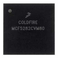
MCF5282CVM80 Freescale Semiconductor, MCF5282CVM80 Datasheet - Page 278

MCF5282CVM80
Manufacturer Part Number
MCF5282CVM80
Description
IC MPU 512K 80MHZ 256-MAPBGA
Manufacturer
Freescale Semiconductor
Series
MCF528xr
Datasheet
1.MCF5216CVM66J.pdf
(766 pages)
Specifications of MCF5282CVM80
Core Processor
Coldfire V2
Core Size
32-Bit
Speed
80MHz
Connectivity
CAN, EBI/EMI, Ethernet, I²C, SPI, UART/USART
Peripherals
DMA, LVD, POR, PWM, WDT
Number Of I /o
150
Program Memory Size
512KB (512K x 8)
Program Memory Type
FLASH
Ram Size
64K x 8
Voltage - Supply (vcc/vdd)
2.7 V ~ 3.6 V
Data Converters
A/D 8x10b
Oscillator Type
External
Operating Temperature
-40°C ~ 85°C
Package / Case
256-MAPBGA
Controller Family/series
ColdFire
Ram Memory Size
64KB
Embedded Interface Type
CAN, I2C, SPI, UART
No. Of Pwm Channels
8
Digital Ic Case Style
MAPBGA
Rohs Compliant
Yes
Lead Free Status / RoHS Status
Lead free / RoHS Compliant
Eeprom Size
-
Available stocks
Company
Part Number
Manufacturer
Quantity
Price
Company:
Part Number:
MCF5282CVM80
Manufacturer:
FREESCALE
Quantity:
1 831
Company:
Part Number:
MCF5282CVM80
Manufacturer:
Freescale Semiconductor
Quantity:
10 000
Company:
Part Number:
MCF5282CVM80J
Manufacturer:
Freescale Semiconductor
Quantity:
10 000
- Current page: 278 of 766
- Download datasheet (9Mb)
Synchronous DRAM Controller Module
15.2.2.2 DRAM Address and Control Registers (DACR0/DACR1)
The DACRn registers, shown in
for memory blocks 0 and 1 of the SDRAM controller. Address and timing are also controlled by bits in
DACRn.
Table 15-5
15-6
31–18
17–16
13–12
Address
Bit
15
14
11
Reset
Field
R/W
describes DACRn fields.
Name
CASL CAS latency. Affects the following SDRAM timing specifications. Timing nomenclature varies with
RE
BA
31
—
—
—
Base address register. With DCMR[BAM], determines the address range in which the associated
DRAM block is located. Each BA bit is compared with the corresponding address of the current bus
cycle. If all unmasked bits match, the address hits in the associated DRAM block. BA functions the
same as in asynchronous operation.
Reserved, should be cleared.
Refresh enable. Determines when the DRAM controller generates a refresh cycle to the DRAM block.
0 Do not refresh associated DRAM block
1 Refresh associated DRAM block
Reserved, should be cleared.
manufacturers. Refer to the SDRAM specification for the appropriate timing nomenclature:
Reserved, should be cleared.
t
t
t
t
t
command
t
RCD
CASL
RAS
RP
RWL
EP
—Last data out to precharge command
—Precharge command to
—
—SRAS assertion to SCAS assertion
,
Figure 15-3. DRAM Address and Control Register (DACRn)
t
—SCAS assertion to data out
RDL
MCF5282 and MCF5216 ColdFire Microcontroller User’s Manual, Rev. 3
ACTV
—Last data input to precharge
Uninitialized
BA
command to precharge command
Figure
Table 15-5. DACRn Field Descriptions
Parameter
IPSBAR+0x048 (DACR0); 0x050 (DACR1)
15-3, contain the base address compare value and the control bits
ACTV
18 17 16 15 14 13 12 11 10 9
command
—
Description
RE — CASL —
R/W
0
CASL= 00 CASL = 01 CASL= 10 CASL= 11
Uninitialized
1
1
2
1
1
1
Number of Bus Clocks
CBM
2
2
4
2
1
1
8
— IMRS PS IP
7
0
6
Freescale Semiconductor
3
3
6
3
1
1
5
Uninitialized
4
3
2
1
—
3
3
6
3
1
0
Related parts for MCF5282CVM80
Image
Part Number
Description
Manufacturer
Datasheet
Request
R
Part Number:
Description:
Mcf5282 And Mcf5216 Coldfire Microcontroller User�s Manual
Manufacturer:
Freescale Semiconductor, Inc
Datasheet:
Part Number:
Description:
Manufacturer:
Freescale Semiconductor, Inc
Datasheet:
Part Number:
Description:
Manufacturer:
Freescale Semiconductor, Inc
Datasheet:
Part Number:
Description:
Manufacturer:
Freescale Semiconductor, Inc
Datasheet:
Part Number:
Description:
Manufacturer:
Freescale Semiconductor, Inc
Datasheet:
Part Number:
Description:
Manufacturer:
Freescale Semiconductor, Inc
Datasheet:
Part Number:
Description:
Manufacturer:
Freescale Semiconductor, Inc
Datasheet:
Part Number:
Description:
Manufacturer:
Freescale Semiconductor, Inc
Datasheet:
Part Number:
Description:
Manufacturer:
Freescale Semiconductor, Inc
Datasheet:
Part Number:
Description:
Manufacturer:
Freescale Semiconductor, Inc
Datasheet:
Part Number:
Description:
Manufacturer:
Freescale Semiconductor, Inc
Datasheet:
Part Number:
Description:
Manufacturer:
Freescale Semiconductor, Inc
Datasheet:
Part Number:
Description:
Manufacturer:
Freescale Semiconductor, Inc
Datasheet:
Part Number:
Description:
Manufacturer:
Freescale Semiconductor, Inc
Datasheet:
Part Number:
Description:
Manufacturer:
Freescale Semiconductor, Inc
Datasheet:


