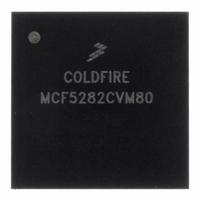
MCF5282CVM80 Freescale Semiconductor, MCF5282CVM80 Datasheet - Page 536

MCF5282CVM80
Manufacturer Part Number
MCF5282CVM80
Description
IC MPU 512K 80MHZ 256-MAPBGA
Manufacturer
Freescale Semiconductor
Series
MCF528xr
Datasheet
1.MCF5216CVM66J.pdf
(766 pages)
Specifications of MCF5282CVM80
Core Processor
Coldfire V2
Core Size
32-Bit
Speed
80MHz
Connectivity
CAN, EBI/EMI, Ethernet, I²C, SPI, UART/USART
Peripherals
DMA, LVD, POR, PWM, WDT
Number Of I /o
150
Program Memory Size
512KB (512K x 8)
Program Memory Type
FLASH
Ram Size
64K x 8
Voltage - Supply (vcc/vdd)
2.7 V ~ 3.6 V
Data Converters
A/D 8x10b
Oscillator Type
External
Operating Temperature
-40°C ~ 85°C
Package / Case
256-MAPBGA
Controller Family/series
ColdFire
Ram Memory Size
64KB
Embedded Interface Type
CAN, I2C, SPI, UART
No. Of Pwm Channels
8
Digital Ic Case Style
MAPBGA
Rohs Compliant
Yes
Lead Free Status / RoHS Status
Lead free / RoHS Compliant
Eeprom Size
-
Available stocks
Company
Part Number
Manufacturer
Quantity
Price
Company:
Part Number:
MCF5282CVM80
Manufacturer:
FREESCALE
Quantity:
1 831
Company:
Part Number:
MCF5282CVM80
Manufacturer:
Freescale Semiconductor
Quantity:
10 000
Company:
Part Number:
MCF5282CVM80J
Manufacturer:
Freescale Semiconductor
Quantity:
10 000
- Current page: 536 of 766
- Download datasheet (9Mb)
Chip Configuration Module (CCM)
27.6.2
The chip mode is selected during reset and reflected in the MODE field of the chip configuration register
(CCR). See
mode cannot be changed.
27-8
1
2
3
4
5
Modifying the default configurations is possible only if the external RCON pin is asserted.
The D[31:27, 23:22, 20, 15:0] pins do not affect reset configuration.
The external reset override circuitry drives the data bus pins with the override values while RSTO is asserted. It must stop
driving the data bus pins within one CLKOUT cycle after RSTO is negated. To prevent contention with the external reset
override circuitry, the reset override pins are forced to inputs during reset and do not become outputs until at least one
CLKOUT cycle after RSTO is negated.
RCON[0] has higher priority than RCON[3:2]. When RCON[0] is configured to boot the chip in single chip mode, the part will
boot internally with a 32-bit port overriding any configuration set by RCON[3:2].
Default configuration
A[23:21]/CS[6:4]
Pin(s) Affected
All output pins
Clock mode
Chip Mode Selection
CS0
Section 27.5.3.1, “Chip Configuration Register
MCF5282 and MCF5216 ColdFire Microcontroller User’s Manual, Rev. 3
Table 27-9
Table 27-8. Configuration During Reset
RCON[4:3] = 00
RCON[9:8] = 00
Configuration
RCON2 = 0
RCON5 = 1
Default
N/A
shows the mode selection during reset configuration.
CLKMOD1, CLKMOD0
Override Pins
in Reset
D[19:18]
D[25:24]
D21
00
10
01
11
00
01
10
11
00
10
01
11
0
1
2,34
(CCR).” Once reset is exited, the operating
1
(continued)
Normal PLL mode w/crystal reference
External clock mode (PLL disabled)
PF[7:6] = CS6, CS5 / PF[5] = A[21]
PF[7] = CS6 / PF[6:5] = A[22:21]
Normal PLL mode with external
Output Pad Drive Strength
Chip Select Configuration
PF[7:6] = CS6, CS5, CS4
Internal with 32-bit port
External with 16-bit port
External with 32-bit port
External with 8-bit port
PF[7:5] = A[23:21]
Partial strength
clock reference
1:1 PLL mode
Full strength
Boot Device
Clock Mode
Function
Freescale Semiconductor
5
5
5
Related parts for MCF5282CVM80
Image
Part Number
Description
Manufacturer
Datasheet
Request
R
Part Number:
Description:
Mcf5282 And Mcf5216 Coldfire Microcontroller User�s Manual
Manufacturer:
Freescale Semiconductor, Inc
Datasheet:
Part Number:
Description:
Manufacturer:
Freescale Semiconductor, Inc
Datasheet:
Part Number:
Description:
Manufacturer:
Freescale Semiconductor, Inc
Datasheet:
Part Number:
Description:
Manufacturer:
Freescale Semiconductor, Inc
Datasheet:
Part Number:
Description:
Manufacturer:
Freescale Semiconductor, Inc
Datasheet:
Part Number:
Description:
Manufacturer:
Freescale Semiconductor, Inc
Datasheet:
Part Number:
Description:
Manufacturer:
Freescale Semiconductor, Inc
Datasheet:
Part Number:
Description:
Manufacturer:
Freescale Semiconductor, Inc
Datasheet:
Part Number:
Description:
Manufacturer:
Freescale Semiconductor, Inc
Datasheet:
Part Number:
Description:
Manufacturer:
Freescale Semiconductor, Inc
Datasheet:
Part Number:
Description:
Manufacturer:
Freescale Semiconductor, Inc
Datasheet:
Part Number:
Description:
Manufacturer:
Freescale Semiconductor, Inc
Datasheet:
Part Number:
Description:
Manufacturer:
Freescale Semiconductor, Inc
Datasheet:
Part Number:
Description:
Manufacturer:
Freescale Semiconductor, Inc
Datasheet:
Part Number:
Description:
Manufacturer:
Freescale Semiconductor, Inc
Datasheet:


