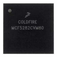
MCF5282CVM80 Freescale Semiconductor, MCF5282CVM80 Datasheet - Page 636

MCF5282CVM80
Manufacturer Part Number
MCF5282CVM80
Description
IC MPU 512K 80MHZ 256-MAPBGA
Manufacturer
Freescale Semiconductor
Series
MCF528xr
Datasheet
1.MCF5216CVM66J.pdf
(766 pages)
Specifications of MCF5282CVM80
Core Processor
Coldfire V2
Core Size
32-Bit
Speed
80MHz
Connectivity
CAN, EBI/EMI, Ethernet, I²C, SPI, UART/USART
Peripherals
DMA, LVD, POR, PWM, WDT
Number Of I /o
150
Program Memory Size
512KB (512K x 8)
Program Memory Type
FLASH
Ram Size
64K x 8
Voltage - Supply (vcc/vdd)
2.7 V ~ 3.6 V
Data Converters
A/D 8x10b
Oscillator Type
External
Operating Temperature
-40°C ~ 85°C
Package / Case
256-MAPBGA
Controller Family/series
ColdFire
Ram Memory Size
64KB
Embedded Interface Type
CAN, I2C, SPI, UART
No. Of Pwm Channels
8
Digital Ic Case Style
MAPBGA
Rohs Compliant
Yes
Lead Free Status / RoHS Status
Lead free / RoHS Compliant
Eeprom Size
-
Available stocks
Company
Part Number
Manufacturer
Quantity
Price
Company:
Part Number:
MCF5282CVM80
Manufacturer:
FREESCALE
Quantity:
1 831
Company:
Part Number:
MCF5282CVM80
Manufacturer:
Freescale Semiconductor
Quantity:
10 000
Company:
Part Number:
MCF5282CVM80J
Manufacturer:
Freescale Semiconductor
Quantity:
10 000
- Current page: 636 of 766
- Download datasheet (9Mb)
Debug Support
30.5.2
When the CPU is halted and PST reflects the halt status, the development system can send unrestricted
commands to the debug module. The debug module implements a synchronous protocol using two inputs
(DSCLK and DSI) and one output (DSO), where DSO is specified as a delay relative to the rising edge of
the processor clock. See
master and must generate DSCLK.
The serial channel operates at a frequency from DC to 1/5 of the CLKOUT frequency. The channel uses
full-duplex mode, where data is sent and received simultaneously by both master and slave devices. The
transmission consists of 17-bit packets composed of a status/control bit and a 16-bit data word. As shown
in
is, DSI is sampled and DSO is driven.
DSCLK and DSI are synchronized inputs. DSCLK acts as a pseudo clock enable and is sampled on the
rising edge of the processor clock as well as the DSI. DSO is delayed from the DSCLK-enabled CLK rising
edge (registered after a BDM state machine state change). All events in the debug module’s serial state
machine are based on the processor clock rising edge. DSCLK must also be sampled low (on a positive
edge of CLK) between each bit exchange. The MSB is transferred first. Because DSO changes state based
on an internally-recognized rising edge of DSCLK, DSDO cannot be used to indicate the start of a serial
transfer. The development system must count clock cycles in a given transfer. C1–C4 are described as
follows:
30.5.2.1 Receive Packet Format
The basic receive packet,
30-18
Figure
•
•
•
•
C1—First synchronization cycle for DSI (DSCLK is high).
C2—Second synchronization cycle for DSI (DSCLK is high).
C3—BDM state machine changes state depending upon DSI and whether the entire input data
transfer has been transmitted.
C4—DSO changes to next value.
BDM State
30-12, all state transitions are enabled on a rising edge of CLKOUT when DSCLK is high; that
CLKOUT
BDM Serial Interface
Machine
DSCLK
DSO
A not-ready response can be ignored except during a memory-referencing
cycle. Otherwise, the debug module can accept a new serial transfer after 32
processor clock periods.
DSI
MCF5282 and MCF5216 ColdFire Microcontroller User’s Manual, Rev. 3
Table
Figure
30-1. The development system serves as the serial communication channel
Current State
Figure 30-12. BDM Serial Interface Timing
30-13, consists of 16 data bits and 1 status bit
Past
C1
Current
C2
NOTE
C3
C4
Next State
Current
Next
Freescale Semiconductor
Related parts for MCF5282CVM80
Image
Part Number
Description
Manufacturer
Datasheet
Request
R
Part Number:
Description:
Mcf5282 And Mcf5216 Coldfire Microcontroller User�s Manual
Manufacturer:
Freescale Semiconductor, Inc
Datasheet:
Part Number:
Description:
Manufacturer:
Freescale Semiconductor, Inc
Datasheet:
Part Number:
Description:
Manufacturer:
Freescale Semiconductor, Inc
Datasheet:
Part Number:
Description:
Manufacturer:
Freescale Semiconductor, Inc
Datasheet:
Part Number:
Description:
Manufacturer:
Freescale Semiconductor, Inc
Datasheet:
Part Number:
Description:
Manufacturer:
Freescale Semiconductor, Inc
Datasheet:
Part Number:
Description:
Manufacturer:
Freescale Semiconductor, Inc
Datasheet:
Part Number:
Description:
Manufacturer:
Freescale Semiconductor, Inc
Datasheet:
Part Number:
Description:
Manufacturer:
Freescale Semiconductor, Inc
Datasheet:
Part Number:
Description:
Manufacturer:
Freescale Semiconductor, Inc
Datasheet:
Part Number:
Description:
Manufacturer:
Freescale Semiconductor, Inc
Datasheet:
Part Number:
Description:
Manufacturer:
Freescale Semiconductor, Inc
Datasheet:
Part Number:
Description:
Manufacturer:
Freescale Semiconductor, Inc
Datasheet:
Part Number:
Description:
Manufacturer:
Freescale Semiconductor, Inc
Datasheet:
Part Number:
Description:
Manufacturer:
Freescale Semiconductor, Inc
Datasheet:


