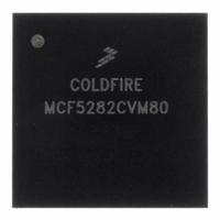
MCF5282CVM80 Freescale Semiconductor, MCF5282CVM80 Datasheet - Page 54

MCF5282CVM80
Manufacturer Part Number
MCF5282CVM80
Description
IC MPU 512K 80MHZ 256-MAPBGA
Manufacturer
Freescale Semiconductor
Series
MCF528xr
Datasheet
1.MCF5216CVM66J.pdf
(766 pages)
Specifications of MCF5282CVM80
Core Processor
Coldfire V2
Core Size
32-Bit
Speed
80MHz
Connectivity
CAN, EBI/EMI, Ethernet, I²C, SPI, UART/USART
Peripherals
DMA, LVD, POR, PWM, WDT
Number Of I /o
150
Program Memory Size
512KB (512K x 8)
Program Memory Type
FLASH
Ram Size
64K x 8
Voltage - Supply (vcc/vdd)
2.7 V ~ 3.6 V
Data Converters
A/D 8x10b
Oscillator Type
External
Operating Temperature
-40°C ~ 85°C
Package / Case
256-MAPBGA
Controller Family/series
ColdFire
Ram Memory Size
64KB
Embedded Interface Type
CAN, I2C, SPI, UART
No. Of Pwm Channels
8
Digital Ic Case Style
MAPBGA
Rohs Compliant
Yes
Lead Free Status / RoHS Status
Lead free / RoHS Compliant
Eeprom Size
-
Available stocks
Company
Part Number
Manufacturer
Quantity
Price
Company:
Part Number:
MCF5282CVM80
Manufacturer:
FREESCALE
Quantity:
1 831
Company:
Part Number:
MCF5282CVM80
Manufacturer:
Freescale Semiconductor
Quantity:
10 000
Company:
Part Number:
MCF5282CVM80J
Manufacturer:
Freescale Semiconductor
Quantity:
10 000
- Current page: 54 of 766
- Download datasheet (9Mb)
ColdFire Core
2.2.9
The SR stores the processor status and includes the CCR, the interrupt priority mask, and other control
bits. In supervisor mode, software can access the entire SR. In user mode, only the lower 8 bits (CCR) are
accessible. The control bits indicate the following states for the processor: trace mode (T bit), supervisor
or user mode (S bit), and master or interrupt state (M bit). All defined bits in the SR have read/write access
when in supervisor mode. The lower byte of the SR (the CCR) must be loaded explicitly after reset and
before any compare (CMP), Bcc, or Scc instructions execute.
2-8
2.2.10
The memory base address registers are used to specify the base address of the internal SRAM and flash
modules and indicate the types of references mapped to each. Each base address register includes a base
address, write-protect bit, address space mask bits, and an enable bit. FLASHBAR determines the base
address of the on-chip flash, and RAMBAR determines the base address of the on-chip RAM. For more
information, refer to
“Flash Base Address Register
Field
10–8
CCR
7–0
Reset
BDM: 0x80E (SR)
15
14
13
12
11
M
T
S
I
W
R
Trace enable. When set, the processor performs a trace exception after every instruction.
Reserved, must be cleared.
Supervisor/user state.
0 User mode
1 Supervisor mode
Master/interrupt state. Bit is cleared by an interrupt exception and software can set it during execution of the RTE or
move to SR instructions.
Reserved, must be cleared.
Interrupt level mask. Defines current interrupt level. Interrupt requests are inhibited for all priority levels less than or
equal to current level, except edge-sensitive level 7 requests, which cannot be masked.
Refer to
15
T
0
Status Register (SR)
Memory Base Address Registers (RAMBAR, FLASHBAR)
14
Section 2.2.4, “Condition Code Register
0
0
Section 5.3.1, “SRAM Base Address Register (RAMBAR)”
13
S
1
MCF5282 and MCF5216 ColdFire Microcontroller User’s Manual, Rev. 3
System Byte
12
M
0
(FLASHBAR)”.
11
0
0
Table 2-3. SR Field Descriptions
Figure 2-8. Status Register (SR)
10
1
1
9
I
(CCR)”.
Description
1
8
0
0
7
0
0
6
Condition Code Register (CCR)
0
0
5
—
X
4
Access: Supervisor read/write
and
—
N
3
Freescale Semiconductor
Section 6.3.2,
—
Z
2
BDM read/write
—
V
1
—
C
0
Related parts for MCF5282CVM80
Image
Part Number
Description
Manufacturer
Datasheet
Request
R
Part Number:
Description:
Mcf5282 And Mcf5216 Coldfire Microcontroller User�s Manual
Manufacturer:
Freescale Semiconductor, Inc
Datasheet:
Part Number:
Description:
Manufacturer:
Freescale Semiconductor, Inc
Datasheet:
Part Number:
Description:
Manufacturer:
Freescale Semiconductor, Inc
Datasheet:
Part Number:
Description:
Manufacturer:
Freescale Semiconductor, Inc
Datasheet:
Part Number:
Description:
Manufacturer:
Freescale Semiconductor, Inc
Datasheet:
Part Number:
Description:
Manufacturer:
Freescale Semiconductor, Inc
Datasheet:
Part Number:
Description:
Manufacturer:
Freescale Semiconductor, Inc
Datasheet:
Part Number:
Description:
Manufacturer:
Freescale Semiconductor, Inc
Datasheet:
Part Number:
Description:
Manufacturer:
Freescale Semiconductor, Inc
Datasheet:
Part Number:
Description:
Manufacturer:
Freescale Semiconductor, Inc
Datasheet:
Part Number:
Description:
Manufacturer:
Freescale Semiconductor, Inc
Datasheet:
Part Number:
Description:
Manufacturer:
Freescale Semiconductor, Inc
Datasheet:
Part Number:
Description:
Manufacturer:
Freescale Semiconductor, Inc
Datasheet:
Part Number:
Description:
Manufacturer:
Freescale Semiconductor, Inc
Datasheet:
Part Number:
Description:
Manufacturer:
Freescale Semiconductor, Inc
Datasheet:


