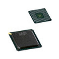
PNX1302EH NXP Semiconductors, PNX1302EH Datasheet - Page 83

PNX1302EH
Manufacturer Part Number
PNX1302EH
Description
Manufacturer
NXP Semiconductors
Datasheet
1.PNX1302EH.pdf
(548 pages)
Specifications of PNX1302EH
Lead Free Status / RoHS Status
Not Compliant
Available stocks
Company
Part Number
Manufacturer
Quantity
Price
Company:
Part Number:
PNX1302EH
Manufacturer:
NXP
Quantity:
201
Part Number:
PNX1302EH
Manufacturer:
PHILIPS/飞利浦
Quantity:
20 000
Company:
Part Number:
PNX1302EH,557
Manufacturer:
NXP Semiconductors
Quantity:
10 000
Company:
Part Number:
PNX1302EH/G
Manufacturer:
NXP
Quantity:
5 510
Part Number:
PNX1302EH/G
Manufacturer:
NXP/恩智浦
Quantity:
20 000
- Current page: 83 of 548
- Download datasheet (6Mb)
Cache Architecture
5.1
In this document, the generic PNX1300 name refers
to the PNX1300 Series, or the PNX1300/01/02/11
products.
The high-performance video and audio throughput of
PNX1300 is implemented by its DSPCPU and autono-
mous I/O and co-processing units, but the foundation of
this processing is the PNX1300 memory hierarchy. To
get the full potential of the chip’s processing units, the
memory hierarchy must read and write data (and DSP
CPU instructions) fast enough to keep the units busy.
To meet the requirements of its target applications,
PNX1300’s memory hierarchy must satisfy the conflict-
ing goals of low cost, simple system design (e.g., low
parts count), and high performance. Since multimedia
video streams can require relatively large temporary
storage, a significant amount of external DRAM is re-
quired. Minimizing the cost of bulk memory is important.
PNX1300’s memory system achieves a good compro-
mise between cost and performance by coupling sub-
stantial on-chip caches with a glueless interface to syn-
chronous DRAM (SDRAM). SDRAM provides higher
bandwidth than standard DRAM for only a small cost pre-
mium. A block diagram of the memory system is shown
in
rower and simpler interface than would be required to
achieve similar performance with standard DRAM.
Figure 5-1. The main components of the PNX1300 memory system.
Figure
MEMORY SYSTEM OVERVIEW
5-1. SDRAM permits PNX1300 to use a nar-
VLIW
CPU
224 bits of decompressed
instruction
Two sets, each has a guard,
opcode, data, and two
address components
Three sets, each has address,
opcode, condition, and guard
Decompressor
Memory
Branch
Three
Units
Units
Two
32KB, 8-way
16KB, 8-way
Instruction
Cache
Cache
Data
The separate on-chip data and instruction caches serve
only the DSPCPU since the data access patterns of the
autonomous I/O and graphics units exhibit little or no lo-
cality of reference (they access each piece of the multi-
media data stream only once in each operation).
Without the caches, the CPU would not be able to
achieve its performance potential. SDRAM has enough
bandwidth to handle serial streams of multimedia data,
but its bandwidth and latency are insufficient to satisfy
the CPU’s high rate of random data accesses and re-
peated instruction accesses.
Table 5-1. 100-MHz PNX1300 memory bandwidth
parameters
Table 5-1
DSPCPU and the main-memory interface. Although 400
MB/s is a lot of bandwidth, it is clear that the SDRAM
alone cannot keep up with the CPU’s maximum require-
ments for instructions and data. Luckily, multimedia algo-
rithms resemble other computer programs in terms of lo-
cality of reference, so the on-chip caches typically supply
To on-chip
peripherals
PRELIMINARY SPECIFICATION
2800 MB/s
800 MB/s
400 MB/s
Magnitude
Internal data highway:
32-bit address, 32-bit
data
shows bandwidth parameters for the PNX1300
Interface
Memory
Main
Instruction bandwidth (224 bits/instruction)
Data bandwidth (two 32-bit memory ports)
Main-memory bandwidth (one 32-bit port)
Chapter 5
Use
Main-memory bus:
glueless, SDRAM
control with 32-bit
data
by Eino Jacobs
Memory
SDRAM
Main
5-1
Related parts for PNX1302EH
Image
Part Number
Description
Manufacturer
Datasheet
Request
R
Part Number:
Description:
NXP Semiconductors designed the LPC2420/2460 microcontroller around a 16-bit/32-bitARM7TDMI-S CPU core with real-time debug interfaces that include both JTAG andembedded trace
Manufacturer:
NXP Semiconductors
Datasheet:

Part Number:
Description:
NXP Semiconductors designed the LPC2458 microcontroller around a 16-bit/32-bitARM7TDMI-S CPU core with real-time debug interfaces that include both JTAG andembedded trace
Manufacturer:
NXP Semiconductors
Datasheet:
Part Number:
Description:
NXP Semiconductors designed the LPC2468 microcontroller around a 16-bit/32-bitARM7TDMI-S CPU core with real-time debug interfaces that include both JTAG andembedded trace
Manufacturer:
NXP Semiconductors
Datasheet:
Part Number:
Description:
NXP Semiconductors designed the LPC2470 microcontroller, powered by theARM7TDMI-S core, to be a highly integrated microcontroller for a wide range ofapplications that require advanced communications and high quality graphic displays
Manufacturer:
NXP Semiconductors
Datasheet:
Part Number:
Description:
NXP Semiconductors designed the LPC2478 microcontroller, powered by theARM7TDMI-S core, to be a highly integrated microcontroller for a wide range ofapplications that require advanced communications and high quality graphic displays
Manufacturer:
NXP Semiconductors
Datasheet:
Part Number:
Description:
The Philips Semiconductors XA (eXtended Architecture) family of 16-bit single-chip microcontrollers is powerful enough to easily handle the requirements of high performance embedded applications, yet inexpensive enough to compete in the market for hi
Manufacturer:
NXP Semiconductors
Datasheet:
Part Number:
Description:
The XA-S3 device is a member of Philips Semiconductors? XA(eXtended Architecture) family of high performance 16-bitsingle-chip microcontrollers
Manufacturer:
NXP Semiconductors
Datasheet:

Part Number:
Description:
The NXP BlueStreak LH75401/LH75411 family consists of two low-cost 16/32-bit System-on-Chip (SoC) devices
Manufacturer:
NXP Semiconductors
Datasheet:

Part Number:
Description:
The NXP LPC3130/3131 combine an 180 MHz ARM926EJ-S CPU core, high-speed USB2
Manufacturer:
NXP Semiconductors
Datasheet:

Part Number:
Description:
The NXP LPC3141 combine a 270 MHz ARM926EJ-S CPU core, High-speed USB 2
Manufacturer:
NXP Semiconductors

Part Number:
Description:
The NXP LPC3143 combine a 270 MHz ARM926EJ-S CPU core, High-speed USB 2
Manufacturer:
NXP Semiconductors

Part Number:
Description:
The NXP LPC3152 combines an 180 MHz ARM926EJ-S CPU core, High-speed USB 2
Manufacturer:
NXP Semiconductors

Part Number:
Description:
The NXP LPC3154 combines an 180 MHz ARM926EJ-S CPU core, High-speed USB 2
Manufacturer:
NXP Semiconductors

Part Number:
Description:
Standard level N-channel enhancement mode Field-Effect Transistor (FET) in a plastic package using NXP High-Performance Automotive (HPA) TrenchMOS technology
Manufacturer:
NXP Semiconductors
Datasheet:


