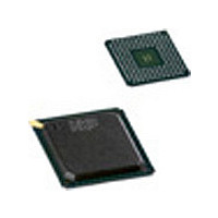
PNX1302EH NXP Semiconductors, PNX1302EH Datasheet - Page 291

PNX1302EH
Manufacturer Part Number
PNX1302EH
Description
Manufacturer
NXP Semiconductors
Datasheet
1.PNX1302EH.pdf
(548 pages)
Specifications of PNX1302EH
Lead Free Status / RoHS Status
Not Compliant
Available stocks
Company
Part Number
Manufacturer
Quantity
Price
Company:
Part Number:
PNX1302EH
Manufacturer:
NXP
Quantity:
201
Part Number:
PNX1302EH
Manufacturer:
PHILIPS/飞利浦
Quantity:
20 000
Company:
Part Number:
PNX1302EH,557
Manufacturer:
NXP Semiconductors
Quantity:
10 000
Company:
Part Number:
PNX1302EH/G
Manufacturer:
NXP
Quantity:
5 510
Part Number:
PNX1302EH/G
Manufacturer:
NXP/恩智浦
Quantity:
20 000
- Current page: 291 of 548
- Download datasheet (6Mb)
Philips Semiconductors
signal so that only one EEPROM chip enable signal is
active at global chip enable time.
22.5
The PCI-XIO Bus Controller has one programmer visible
MMIO register: XIO_CTL. Its format is shown in
Table
any undefined MMIO bits should be ignored when read,
and written as ‘0’s.
Table 22-2. XIO_CTL Register Fields: MMIO Address
0x10 3060
22.5.1
PCI_CLK, the clock for the PCI and PCI-XIO bus can be
supplied externally or internally. This is determined at
Figure 22-9. Multiple 8-bit Flash EEPROM Interface
Address
Wait States
Enable
Clock Fre-
quency
PCI_INTB#
PCI_AD[19-17]
Field
22-2. To ensure compatibility with future devices,
XIO_CTL MMIO REGISTER
PCI_CLK Bus Clock Frequency
+3
31:26
25:11
Bits
10:8
6:5
4:0
7
XIO address space
unused
Wait states
Enable XIO Bus opera-
tion
unused
Clock divider
74FCT138
E2
E1
E0
A[2-0] O0
PCI_C/BE1#: IOWR#
PCI_C/BE0#: IORD#
Function
PCI_AD[16:0]
O1
O2
O3
O4
O5
O6
O7
128-256K
256-384K
384-512K
512-640K
640-768K
768-896K
896-1024K
0-128K
undefined
0
0
0 = disabled
0x1f
Reset Value
Output Enable
Chip Select
Output Enable
Chip Select
Address
Write Enable
Address
Write Enable
boot time, by the ‘enable internal PCI_CLK generator’ bit,
bit 6 of byte 9 in the boot EEPROM. Refer to
on page
with TM-1000 and normal PCI operation, i.e. PCI_CLK is
an input pin that takes the PCI clock from the external
world. If this bit = ‘1’, an on-chip clock divider in the XIO
logic becomes the source of PCI_CLK, and the PCI_CLK
pin is configured as an output. In the latter case, the
PCI_CLK frequency can be programmed to a divider of
the PNX1300 highway clock by setting the XIO_CTL reg-
ister ‘Clock Frequency’ divider value.
Table 22-3. PCI_CLK frequencies for 133.0 MHz
PNX1300 highway clock
PRELIMINARY SPECIFICATION
Frequency
128Kx8 EEPROM
128Kx8 EEPROM
(use odd
values)
Clock
30
31
...
0
1
2
3
13-2. If this bit = ‘0’, PCI_CLK acts compatible
PNX1300
Clocks
illegal
31
32
...
2
3
4
Data
Data
PCI-XIO External I/O Bus
PCI-XIO Clock
Period, ns
illegal
22.5
233
241
15
30
...
PCI_AD[31:24]
Section 13.2
Frequency,
illegal
44.33
33.25
MHz
66.5
4.29
4.16
...
22-7
Related parts for PNX1302EH
Image
Part Number
Description
Manufacturer
Datasheet
Request
R
Part Number:
Description:
NXP Semiconductors designed the LPC2420/2460 microcontroller around a 16-bit/32-bitARM7TDMI-S CPU core with real-time debug interfaces that include both JTAG andembedded trace
Manufacturer:
NXP Semiconductors
Datasheet:

Part Number:
Description:
NXP Semiconductors designed the LPC2458 microcontroller around a 16-bit/32-bitARM7TDMI-S CPU core with real-time debug interfaces that include both JTAG andembedded trace
Manufacturer:
NXP Semiconductors
Datasheet:
Part Number:
Description:
NXP Semiconductors designed the LPC2468 microcontroller around a 16-bit/32-bitARM7TDMI-S CPU core with real-time debug interfaces that include both JTAG andembedded trace
Manufacturer:
NXP Semiconductors
Datasheet:
Part Number:
Description:
NXP Semiconductors designed the LPC2470 microcontroller, powered by theARM7TDMI-S core, to be a highly integrated microcontroller for a wide range ofapplications that require advanced communications and high quality graphic displays
Manufacturer:
NXP Semiconductors
Datasheet:
Part Number:
Description:
NXP Semiconductors designed the LPC2478 microcontroller, powered by theARM7TDMI-S core, to be a highly integrated microcontroller for a wide range ofapplications that require advanced communications and high quality graphic displays
Manufacturer:
NXP Semiconductors
Datasheet:
Part Number:
Description:
The Philips Semiconductors XA (eXtended Architecture) family of 16-bit single-chip microcontrollers is powerful enough to easily handle the requirements of high performance embedded applications, yet inexpensive enough to compete in the market for hi
Manufacturer:
NXP Semiconductors
Datasheet:
Part Number:
Description:
The XA-S3 device is a member of Philips Semiconductors? XA(eXtended Architecture) family of high performance 16-bitsingle-chip microcontrollers
Manufacturer:
NXP Semiconductors
Datasheet:

Part Number:
Description:
The NXP BlueStreak LH75401/LH75411 family consists of two low-cost 16/32-bit System-on-Chip (SoC) devices
Manufacturer:
NXP Semiconductors
Datasheet:

Part Number:
Description:
The NXP LPC3130/3131 combine an 180 MHz ARM926EJ-S CPU core, high-speed USB2
Manufacturer:
NXP Semiconductors
Datasheet:

Part Number:
Description:
The NXP LPC3141 combine a 270 MHz ARM926EJ-S CPU core, High-speed USB 2
Manufacturer:
NXP Semiconductors

Part Number:
Description:
The NXP LPC3143 combine a 270 MHz ARM926EJ-S CPU core, High-speed USB 2
Manufacturer:
NXP Semiconductors

Part Number:
Description:
The NXP LPC3152 combines an 180 MHz ARM926EJ-S CPU core, High-speed USB 2
Manufacturer:
NXP Semiconductors

Part Number:
Description:
The NXP LPC3154 combines an 180 MHz ARM926EJ-S CPU core, High-speed USB 2
Manufacturer:
NXP Semiconductors

Part Number:
Description:
Standard level N-channel enhancement mode Field-Effect Transistor (FET) in a plastic package using NXP High-Performance Automotive (HPA) TrenchMOS technology
Manufacturer:
NXP Semiconductors
Datasheet:


