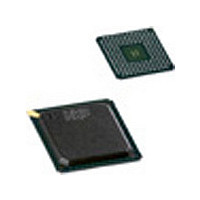
PNX1302EH NXP Semiconductors, PNX1302EH Datasheet - Page 27

PNX1302EH
Manufacturer Part Number
PNX1302EH
Description
Manufacturer
NXP Semiconductors
Datasheet
1.PNX1302EH.pdf
(548 pages)
Specifications of PNX1302EH
Lead Free Status / RoHS Status
Not Compliant
Available stocks
Company
Part Number
Manufacturer
Quantity
Price
Company:
Part Number:
PNX1302EH
Manufacturer:
NXP
Quantity:
201
Part Number:
PNX1302EH
Manufacturer:
PHILIPS/飞利浦
Quantity:
20 000
Company:
Part Number:
PNX1302EH,557
Manufacturer:
NXP Semiconductors
Quantity:
10 000
Company:
Part Number:
PNX1302EH/G
Manufacturer:
NXP
Quantity:
5 510
Part Number:
PNX1302EH/G
Manufacturer:
NXP/恩智浦
Quantity:
20 000
- Current page: 27 of 548
- Download datasheet (6Mb)
Pin List
1.1
The following summarizes differences between TM-1300 and PNX1300/01/02/11:
• Lower core voltage for PNX1311 (2.2V core voltage) and therefore lower power consumption.
• DSPCPU speed of up to 200 MHz.
• SDRAM speed of up to 183 MHz.
• Support for 256 Mbit SDRAM organized in x16. The REFRESH counter must be changed. Refer for in
• Support for 16- and 32-bit Main Memory Interface.
• Simplified power supplies sequencing (see
• Additional mode where VI_DATA[9:8] in message passing mode are not affected by the VI_DVALID signal.
• Bug fixed for PCI Special Cycles. PNX1300 Series discards PCI Special Cycles issued by some PCI chipsets.
• Autonomous boot bug in non 1:1 ratio is fixed, resulting in 2KB boot EEPROM size for all CPU:SDRAM ratios.
In the document, ‘PNX1300 Series’ is used interchangebly with ‘PNX1300/01/02/11’, and it always refers to
PNX1300, PNX1301, PNX1302 and PNX1311 products. Any exception will be noted.
1.2
PNX1300 Series implements full IEEE 1149.1 boundary scan. Any PNX1300 Series pin designated “IN” only (from a
functionality point of view) can become an output during boundary scan.
1.3
PNX1300 Series has a total of 169 functional pins, excluding VDDQ, VSSQ, VREF_PCI and VREF_PERIPH and digital
power/ground. PNX1300 Series uses the types of I/O circuits shown in the table below.
For the pins with 5-V input capability, the special pins VREF_PCI or VREF_PERIPH determine 3.3- or 5-V input toler-
ance, as per the table in
Unused pins may remain floating, i.e. unconnected.
All pins that drive a clock should drive a series resistor.
“SDRAM Memory System”
Pad Type
PCI
PCIOD
IICOD
STRG3
NORM3
STRG5
WEAK5
IN
OUT
OD
I/O
I/OD
PNX1300 SERIES VERSUS TM-1300
BOUNDARY SCAN NOTICE
I/O CIRCUIT SUMMARY
Modes
Input only, except during boundary scan
Output only, except during boundary scan
Open drain output - active pull low, no active drive high, requires external pull-up
Output or input
Open drain output with input - active pull low, no active drive high, requires external pull-up
PCI2.1 compliant I/O, capable of using 3.3-V or 5-V PCI signaling conventions.
PCI2.1 compliant Open Drain I/O, capable of using 3.3-V or 5-V PCI signaling conventions.
Open drain 3.3-V or 5-V I
3.3-V only low impedance I/O. Requires board level 27-33 ohm series terminator resistor to match 50 ohm
PCB trace.
3.3-V only I/O circuit with regular drive strength and board trace matched drive impedance.
3.3-V low impedance output, combined with 5-V tolerant input. If used as output, it requires a board level
27-33 ohm series terminator resistor to match 50-ohm PCB trace.
3.3-V regular impedance output, with slow rise/fall, combined with 5-V tolerant input.
Section
for details.
1.6. The above pad types are used in the modes listed in the following table.
2
C I/O (for I
by John Chang, Wenyi Song, Thorwald Rabeler, Luis Lucas
Section
2
C pins).
Pad Type Description
1.9.4).
Description
PRELIMINARY SPECIFICATION
Chapter 1
Chapter 12,
1-1
Related parts for PNX1302EH
Image
Part Number
Description
Manufacturer
Datasheet
Request
R
Part Number:
Description:
NXP Semiconductors designed the LPC2420/2460 microcontroller around a 16-bit/32-bitARM7TDMI-S CPU core with real-time debug interfaces that include both JTAG andembedded trace
Manufacturer:
NXP Semiconductors
Datasheet:

Part Number:
Description:
NXP Semiconductors designed the LPC2458 microcontroller around a 16-bit/32-bitARM7TDMI-S CPU core with real-time debug interfaces that include both JTAG andembedded trace
Manufacturer:
NXP Semiconductors
Datasheet:
Part Number:
Description:
NXP Semiconductors designed the LPC2468 microcontroller around a 16-bit/32-bitARM7TDMI-S CPU core with real-time debug interfaces that include both JTAG andembedded trace
Manufacturer:
NXP Semiconductors
Datasheet:
Part Number:
Description:
NXP Semiconductors designed the LPC2470 microcontroller, powered by theARM7TDMI-S core, to be a highly integrated microcontroller for a wide range ofapplications that require advanced communications and high quality graphic displays
Manufacturer:
NXP Semiconductors
Datasheet:
Part Number:
Description:
NXP Semiconductors designed the LPC2478 microcontroller, powered by theARM7TDMI-S core, to be a highly integrated microcontroller for a wide range ofapplications that require advanced communications and high quality graphic displays
Manufacturer:
NXP Semiconductors
Datasheet:
Part Number:
Description:
The Philips Semiconductors XA (eXtended Architecture) family of 16-bit single-chip microcontrollers is powerful enough to easily handle the requirements of high performance embedded applications, yet inexpensive enough to compete in the market for hi
Manufacturer:
NXP Semiconductors
Datasheet:
Part Number:
Description:
The XA-S3 device is a member of Philips Semiconductors? XA(eXtended Architecture) family of high performance 16-bitsingle-chip microcontrollers
Manufacturer:
NXP Semiconductors
Datasheet:

Part Number:
Description:
The NXP BlueStreak LH75401/LH75411 family consists of two low-cost 16/32-bit System-on-Chip (SoC) devices
Manufacturer:
NXP Semiconductors
Datasheet:

Part Number:
Description:
The NXP LPC3130/3131 combine an 180 MHz ARM926EJ-S CPU core, high-speed USB2
Manufacturer:
NXP Semiconductors
Datasheet:

Part Number:
Description:
The NXP LPC3141 combine a 270 MHz ARM926EJ-S CPU core, High-speed USB 2
Manufacturer:
NXP Semiconductors

Part Number:
Description:
The NXP LPC3143 combine a 270 MHz ARM926EJ-S CPU core, High-speed USB 2
Manufacturer:
NXP Semiconductors

Part Number:
Description:
The NXP LPC3152 combines an 180 MHz ARM926EJ-S CPU core, High-speed USB 2
Manufacturer:
NXP Semiconductors

Part Number:
Description:
The NXP LPC3154 combines an 180 MHz ARM926EJ-S CPU core, High-speed USB 2
Manufacturer:
NXP Semiconductors

Part Number:
Description:
Standard level N-channel enhancement mode Field-Effect Transistor (FET) in a plastic package using NXP High-Performance Automotive (HPA) TrenchMOS technology
Manufacturer:
NXP Semiconductors
Datasheet:


