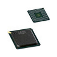
PNX1302EH NXP Semiconductors, PNX1302EH Datasheet - Page 69

PNX1302EH
Manufacturer Part Number
PNX1302EH
Description
Manufacturer
NXP Semiconductors
Datasheet
1.PNX1302EH.pdf
(548 pages)
Specifications of PNX1302EH
Lead Free Status / RoHS Status
Not Compliant
Available stocks
Company
Part Number
Manufacturer
Quantity
Price
Company:
Part Number:
PNX1302EH
Manufacturer:
NXP
Quantity:
201
Part Number:
PNX1302EH
Manufacturer:
PHILIPS/飞利浦
Quantity:
20 000
Company:
Part Number:
PNX1302EH,557
Manufacturer:
NXP Semiconductors
Quantity:
10 000
Company:
Part Number:
PNX1302EH/G
Manufacturer:
NXP
Quantity:
5 510
Part Number:
PNX1302EH/G
Manufacturer:
NXP/恩智浦
Quantity:
20 000
- Current page: 69 of 548
- Download datasheet (6Mb)
Philips Semiconductors
Figure 3-10. Timer register definitions.
Table 3-11. Timer base MMIO address
Table 3-12. Timer source selections
the counter will have to loop around before an interrupt is
generated.
A modulus value of zero causes a wrap-around as if the
modulus value was 2
On RESET, the TCTL registers are cleared, and the val-
ue of the TMODULUS and TVALUE registers is unde-
fined.
TIMER1
TIMER2
TIMER3
SYSTIMER
CLOCK
PRESCALE
TRI_TIMER_CLK
DATABREAK
INSTBREAK
CACHE1
CACHE2
VI_CLK
VO_CLK
AI_WS
AO_WS
SSI_RXFSX
SSI_IO2
—
Timer base offset:
Source Name
0
4
8
TMODULUS (r/w)
TVALUE (r/w)
TCTL (r/w)
MMIO_BASE+0x10,0C60
MMIO_BASE+0x10,0C00
MMIO_BASE+0x10,0C20
MMIO_BASE+0x10,0C40
Source
Value
13-15
Bits
32
10
12
11
0
1
2
3
4
5
6
7
8
9
.
CPU clock
prescaled CPU clock
external clock pin
data breakpoints
instruction breakpoints
cache event 1
cache event 2
video in clock pin
video out clock pin
audio in word strobe pin
audio out word strobe pin
SSI receive frame sync pin
SSI transmit frame sync pin
undefined
Source Description
31
“PRESCALE”:
Prescale value is
2^PRESCALE, i.e.,
in the range [1..32768]
27
23
3.9
This section describes the special debug support offered
by the DSPCPU. Instruction and data breakpoints can be
defined through a set of registers in the MMIO register
space. When a breakpoint is matched, an event is gen-
erated that can be used as a timer source (see
3.8,
generate a DSPCPU interrupt after the desired number
of breakpoint matches.
3.9.1
The instruction-breakpoint control register is shown in
Figure
(MMIO-register addresses shown are offset with respect
to MMIO_BASE.)
The instruction-breakpoint address-range registers are
shown in
registers is undefined. (MMIO-register addresses shown
are offset with respect to MMIO_BASE.)
When the IC bit in the breakpoint control register is set to
‘1’, instruction breakpoints are activated. Any instruction
address issued by the PNX1300 chip is compared
against the low and high address-range values. The IAC
bit in the breakpoint control register determines whether
the instruction address needs to be inside or outside of
the range defined by the low and high address-range
registers. A successful comparison takes place when ei-
ther:
•
•
On a successful comparison, an instruction breakpoint
event is generated, which can be used as a clock input
to a timer. After counting the programmed number of in-
struction breakpoint events, the timer will generate an in-
terrupt request.
PRELIMINARY SPECIFICATION
IAC = ‘0’ and low ≤ iaddr ≤ high, or
IAC = ‘1’ and iaddr < low or iaddr > high.
“Timers”). The timer TMODULUS has to be set to
19
PRESCALE
3-11. On RESET, the BICTL register is cleared.
DEBUG SUPPORT
MODULUS
“SOURCE” select:
see table
Figure
Instruction Breakpoints
VALUE
15
3-12. After RESET, the value of these
Table 3-12
11
SOURCE
DSPCPU Architecture
7
“RUN” bit:
0
1
Timer stopped
Timer running
3
Section
R
0
3-13
Related parts for PNX1302EH
Image
Part Number
Description
Manufacturer
Datasheet
Request
R
Part Number:
Description:
NXP Semiconductors designed the LPC2420/2460 microcontroller around a 16-bit/32-bitARM7TDMI-S CPU core with real-time debug interfaces that include both JTAG andembedded trace
Manufacturer:
NXP Semiconductors
Datasheet:

Part Number:
Description:
NXP Semiconductors designed the LPC2458 microcontroller around a 16-bit/32-bitARM7TDMI-S CPU core with real-time debug interfaces that include both JTAG andembedded trace
Manufacturer:
NXP Semiconductors
Datasheet:
Part Number:
Description:
NXP Semiconductors designed the LPC2468 microcontroller around a 16-bit/32-bitARM7TDMI-S CPU core with real-time debug interfaces that include both JTAG andembedded trace
Manufacturer:
NXP Semiconductors
Datasheet:
Part Number:
Description:
NXP Semiconductors designed the LPC2470 microcontroller, powered by theARM7TDMI-S core, to be a highly integrated microcontroller for a wide range ofapplications that require advanced communications and high quality graphic displays
Manufacturer:
NXP Semiconductors
Datasheet:
Part Number:
Description:
NXP Semiconductors designed the LPC2478 microcontroller, powered by theARM7TDMI-S core, to be a highly integrated microcontroller for a wide range ofapplications that require advanced communications and high quality graphic displays
Manufacturer:
NXP Semiconductors
Datasheet:
Part Number:
Description:
The Philips Semiconductors XA (eXtended Architecture) family of 16-bit single-chip microcontrollers is powerful enough to easily handle the requirements of high performance embedded applications, yet inexpensive enough to compete in the market for hi
Manufacturer:
NXP Semiconductors
Datasheet:
Part Number:
Description:
The XA-S3 device is a member of Philips Semiconductors? XA(eXtended Architecture) family of high performance 16-bitsingle-chip microcontrollers
Manufacturer:
NXP Semiconductors
Datasheet:

Part Number:
Description:
The NXP BlueStreak LH75401/LH75411 family consists of two low-cost 16/32-bit System-on-Chip (SoC) devices
Manufacturer:
NXP Semiconductors
Datasheet:

Part Number:
Description:
The NXP LPC3130/3131 combine an 180 MHz ARM926EJ-S CPU core, high-speed USB2
Manufacturer:
NXP Semiconductors
Datasheet:

Part Number:
Description:
The NXP LPC3141 combine a 270 MHz ARM926EJ-S CPU core, High-speed USB 2
Manufacturer:
NXP Semiconductors

Part Number:
Description:
The NXP LPC3143 combine a 270 MHz ARM926EJ-S CPU core, High-speed USB 2
Manufacturer:
NXP Semiconductors

Part Number:
Description:
The NXP LPC3152 combines an 180 MHz ARM926EJ-S CPU core, High-speed USB 2
Manufacturer:
NXP Semiconductors

Part Number:
Description:
The NXP LPC3154 combines an 180 MHz ARM926EJ-S CPU core, High-speed USB 2
Manufacturer:
NXP Semiconductors

Part Number:
Description:
Standard level N-channel enhancement mode Field-Effect Transistor (FET) in a plastic package using NXP High-Performance Automotive (HPA) TrenchMOS technology
Manufacturer:
NXP Semiconductors
Datasheet:


